
User`s guide


SMPS AC/DC Reference Design User’s Guide
DS70320B-page 44 © 2008 Microchip Technology Inc.
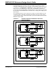
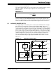
2.4.1 Multi-Phase Buck Converter Power-Train Design
The target specification for the Multi-Phase Buck converter is as follows:
• Input voltage, V
IN = 12 VDC
• Switching frequency, f
sw
= 500 kHz
• Output voltage, V
OUT = 3.3 VDC
• Output power, IOUT = 69 A
• Voltage ripple < 2%
• Output slew rate > 50A/μs
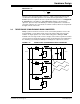
2.4.1.1 MOSFETS AND GATE DRIVE
The output current for each phase Buck stage is 23A and nominal duty cycle is 0.275
ignoring stray voltage drops and inductor current ripple. This equates to a high-side
MOSFET on-time, t
on
, of 550 ns. Therefore, the high-side MOSFET is rated for 12
Arms, and the low-side MOSFET is rated for 19.6A.
The selected MOSFETs are International Rectifier IRLR7833PBF, 30 V, 4.5 mΩ
devices in a DPAK package, and are mounted directly on the PCB. The conduction
losses of the high and low-side MOSFETs are estimated at 0.55W and 1.5W
respectively. The estimated switching transition time is 50 ns, so the switching loss for
each device is 1.2W.
The gate drive circuitry is a dual Microchip MCP1404 gate-drive IC, which drives the
MOSFET gates directly. The maximum gate threshold of each MOSFET is 4V, so the
drive circuit for the high-side MOSFET is provided by the auxiliary SMPS power rail,
which is higher than the gate threshold and source voltage combined. The PWM
module pin of the dsPIC DSC device interfaces with the gate-drive IC via an inverting
open-collector transistor stage which provides immunity against ground bounce.
EQUATION 2-32:
2.4.1.2 OUTPUT CHOKES
The ripple current in each inductor is given by the relationship shown in Equation 2-33.
EQUATION 2-33:
The ripple current needs to be about 20% of the output current; therefore, each output
choke is a 1 μH Coilcraft SER1360-102KL surface mount. The DC resistance is 2.5 mΩ
and the power loss is 1.3W. The peak-to-peak ripple current is 4.8A.
o
bus
V
D
V
=
high o
iID
=
1
low o
iI D
=
−
1
6
s
wbusorsw
P
VItf
=
(
)
0
on bus
tV V
i
L
−
Δ=