
User`s guide


Hardware Design
© 2008 Microchip Technology Inc. DS70320B-page 41
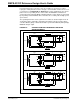
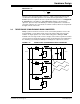
2.3 SINGLE-PHASE SYNCHRONOUS BUCK CONVERTER
The Single-Phase Synchronous Buck converter uses the same basic topology as the
standard step-down Buck converter, but replaces the free-wheel diode with a MOSFET.
Figure 2-11 shows the main power circuitry. The two switches are operated as a
complementary pair with a dead-time inserted by the PWM controller to avoid
shoot-through. The low-side MOSFET is operated in the third quadrant with current
flowing from source to drain when the current is required to free-wheel, and, due to the
very lower ON state resistance of the MOSFET, higher efficiency is achieved compared
with a conventional Schottky diode.
FIGURE 2-11: SINGLE-PHASE SYNCHRONOUS BUCK CONVERTER
2.3.1 Single-Phase Buck Converter Power-Train Design
The target specification for the Single-Phase Buck converter is as follows:
• Input voltage, V
IN = 12 VDC
• Switching frequency, f
sw
= 500 kHz
• Output voltage, V
OUT = 5 VDC
• Output current, IOUT = 23A
• Voltage ripple < 2%
• Output slew rate > 5 A/μs
2.3.1.1 MOSFETS AND GATE DRIVE
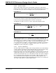
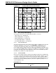
The equation governing the duty cycle of a Buck converter is shown in Equation 2-26.
EQUATION 2-26:
The rms currents in the high-side and low-side MOSFETs, assuming a low inductor
ripple current is as follows in Equation 2-27 and Equation 2-28.
EQUATION 2-27:
V
out
V
bus
o
bus
V
D
V
=
high o
iID
=
%