
User`s guide


Hardware Design
© 2008 Microchip Technology Inc. DS70320B-page 39
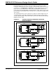
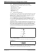
FIGURE 2-10: SYNCHRONOUS RECTIFIER WAVEFORMS
2.2.2.1 MOSFET SYNCHRONOUS RECTIFIERS AND GATE DRIVES
The MOSFET rectifiers selected for the synchronous rectifier are International Rectifier
IRF2804SPBF 40V, 2 mΩ devices. They are packaged in a D
2
PAK and mounted
directly onto the PCB. The minimum blocking voltage required is equal to the peak
applied transformer secondary voltage. With the turns ratio of 12:8 and at the maximum
input voltage of 410V, this is 32V. There will be very little overshoot voltage due to the
compact layout achieved through mounting on the PCB, and the RC snubber across
the secondary winding. The junction to ambient thermal resistance is 40ºC/W when
mounted on a 25.4 mm
2
(1 inch
2
) PCB copper pad (see Reference 11 in Appendix
C. “References”).
The MOSFET’s internal diode voltage characteristic is 0.6V at 30A, 175ºC, which is
significantly above the voltage drop across the 2 mΩ ON state resistance, and the
benefits of synchronous rectification are maintained over the whole operating power
region.
The gate-drive circuit employs a Microchip MCP1403 gate driver. The gate control
signals are generated by the primary-side dsPIC DSC device so that they are
synchronized with the ZVT Full-Bridge commutation. Isolation is achieved by
high-speed opto-isolators.
Q
5
(Q
4
)
Q
6
(Q
2
)
V
SEC
I
SEC
I
1
I
2
t
t
t
t
t
t
t
on
T
I
out
2
I
out
2