
User`s guide

Hardware Design
© 2008 Microchip Technology Inc. DS70320B-page 33
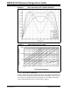
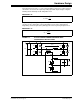
2.2.1 Full-Bridge ZVT Power-Train Design
The target specification for the ZVT Full-Bridge converter is as follows:
• Input voltage, V
IN = 390-420V
• Switching frequency, f
sw
= 250 kHz
• Maximum output voltage, V
OUT = 12V
• Maximum output current, I
OUT = 33A
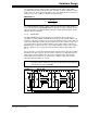
2.2.1.1 MOSFETS AND GATE DRIVE
Care must be taken when selecting the MOSFET switch for the ZVT Full-Bridge since
there are potential failure modes associated with the diode characteristic and timing
control at light loads (see Reference 4 in Appendix C. “References”). For this
reference design, an Infineon CoolMOS CFD device has been selected because of its
optimized diode characteristic. The SPA11N60CFD is a 600V, 0.44Ω MOSFET in a
TO-220 package, and is a good compromise between cost and efficiency for this output
power rating. The output capacitance, C
OSS, is 45 pF and will form the resonant
capacitor for ZVT operation.
Gate driving is typically achieved with either a proprietary high-side and low-side
high-voltage driver IC, or using a small transformer. These circuit techniques provide
level-shifting of the dsPIC DSC gate firing signals. Adequate voltage creepage and
clearance distances are maintained in the layout. Given the high switching frequency
in this application, the transformer isolated gate drive approach has been adopted. This
is because of thermal concerns in standard gate driver ICs, although there are potential
candidates from a number of manufacturers available on the market.
A single drive transformer with two secondary windings manufactured by Sirio
Elettronica is used for each half-limb, and the turn-on switching time is controlled by a
single resistor in each MOSFET gate. Turn-off is much faster due to the diode across
the gate resistor. The drive for each transformer primary is provided by a Microchip
TC1404, which is a dual high-speed CMOS driver IC. The dead-time for each MOSFET
half-limb is inserted by the dsPIC DSC PWM peripheral module and is selected to avoid
any possible shoot-through condition based on the timing delays inherent in the
transformer gate drive circuitry.
2.2.1.2 TRANSFORMER
The following section describes a basic procedure for designing the ZVT Full-Bridge
transformer. The optimum choice of ferrite core and winding turns/construction is
dependent on many factors in the overall converter and may well involve a number of
design optimization iterations.
The transformer turns ratio must be selected to ensure that voltage regulation is
maintained at the maximum duty limit. As a starting point, D
max
is assumed to be 0.85,
so for the minimum DC link voltage (390V) and the output voltage (12.5V), which
includes the voltage drop across the synchronous rectifiers and output chokes, the
required transformer turns ratio is 13.3 or less (see Equation 2-12).
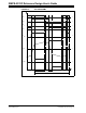
An ungapped ETD29 ferrite core pair is selected for the transformer. Table 2-1 lists the
various parameters for ETD29 cores made of N87 material.
TABLE 2-1: TRANSFORMER CORE DATA
A
L
(nH/Turn
2
)
A
e
(mm
2
)
V
e
(mm
3
)
w
(mm)
h
(mm)
l
m
(mm)
R
th
(ºC/W)
ETD29 2200 76 5350 19.4 4.85 52.8 28