
User`s guide


SMPS AC/DC Reference Design User’s Guide
DS70320B-page 30 © 2008 Microchip Technology Inc.
2.2 FULL-BRIDGE ZVT CONVERTER
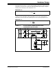
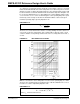
The main power circuit for a ZVT Full-Bridge converter is shown in Figure 2-5. It is a
standard Full-Bridge converter, but with additional series resonant inductance, which
limits the rise rate of current at switching transitions and can eliminate turn-off switching
power dissipation in the MOSFETs. The stray leakage inductance of the transformer
forms part of the series resonant inductor and, in this particular design, is large enough
to ensure quasi-resonant operation over 80% of the operating power range without the
need for an additional inductor. The secondary-side high-frequency rectification is
normally done by using ultrafast recovery rectifiers or Schottky diodes. Alternatively,
lower loss rectification can be achieved by using MOSFETs operating as synchronous
rectifiers with primary-side commutation control, and this is the preferred solution in this
reference design.
ZVT operation occurs when the stored energy in the inductor is transferred to the
capacitor in parallel with the MOSFET. In this design, the stray output capacitance of
the MOSFET is large enough to not require additional capacitors in parallel. From
Reference 3 (see Appendix C. “References”), the equation relating energy in the
MOSFET output capacitance and the series inductance for ZVT operation is given by
Equation 2-9.
EQUATION 2-9:
This ensures that there is more than enough energy to charge the MOSFET output
capacitance and maintain ZVT operation. Note that at low output power, there will be
far less energy stored in the resonant inductance so ZVT operation will be lost. The
inductor is therefore selected based on the minimum operating output power for ZVT
switching.
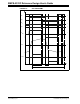
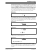
The modulation control scheme required for ZVT operation of a Full-Bridge converter
is phase-shifted PWM. The ideal power stage waveforms for the circuit are shown in
Figure 2-6. The ZVT transition in the switch is short in comparison with the primary
current transition time. This time, Δt, is dictated by the resonant inductance, L
R
, which
is given by Equation 2-10.
EQUATION 2-10:
The control duty cycle is limited in a ZVT due to the time taken for the current to rise/fall
during switching transitions. The maximum duty cycle, D
max
, is achievable under the
ZVT operating conditions given by Equation 2-11.
EQUATION 2-11:
22
14
23
Rpri Rin
L
ICV
≥
2
Rpri
in
L
I
t
V
Δ=
max
2
1
t
D
T
Δ
=−