
User`s guide


SMPS AC/DC Reference Design User’s Guide
DS70320B-page 26 © 2008 Microchip Technology Inc.
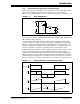
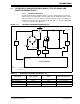
2.1.1 Power-Train Design
The target specification for the PFC converter is as follows:
• Input voltage, V
IN = 85-265 Vrms
• Input frequency, f
in
= 45-65 Hz
• Switching frequency, f
sw
= 125 kHz
• Maximum Output voltage, V
OUT = 420 VDC
• Maximum Output power, POUT = 450 W
• Current THD < 5%
EMC standards for conducted, radiated and line current harmonics:
• FCC Class B
• EN55022 (CISPR 22) Class B
• EN61000-3-2 A14 Class A
• EN61000-3-3
• IEEE519
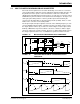
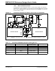
2.1.1.1 MOSFETS AND GATE DRIVE
MOSFETs are the preferred technology for the Boost converter power switch because
of the high operating frequency. The rms current in the MOSFET switch can be
approximated using Equation 2-3.
EQUATION 2-3:
The maximum rms current occurs at minimum mains voltage, so the maximum normal
operating MOSFET current is 4.6 Arms. Therefore, two TO-220 Infineon CoolMOS
™
SPP11N60CFD 500V, 0.44Ω MOSFETs are connected in parallel, with each
dissipating 2.3W of conduction loss. The MOSFET output capacitance is 390 pF so the
switching loss is estimated at about 0.4W each. The actual loss in practice will be layout
dependent and will probably be a factor of 2 higher, but still low enough to achieve high
system efficiency.
The gate drive circuitry is a low-side Microchip TC1412N gate-drive IC, which drives
the MOSFET gates directly. A single dsPIC DSC PWM module pin interfaces with the
gate-drive IC via an inverting open-collector transistor stage which provides immunity
against noise voltage differences between the Boost converter common and dsPIC
DSC signal common (ground bounce).
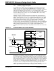
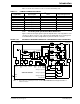
2.1.1.2 OUTPUT DIODE
The output diode must be rated for the mean output current, which is given by
Equation 2-4.
EQUATION 2-4:
16 2
2
3
2
oac
mos
dc
ac
PV
i
V
V
π
=−
%
2
1
2
s
wossdcsw
P
CVf
=
o
diode
dc
P
i
V
=