
User`s guide


SMPS AC/DC REFERENCE
DESIGN USER’S GUIDE
© 2008 Microchip Technology Inc. DS70320B-page iii
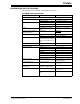
Table of Contents
Preface ........................................................................................................................... 1
Chapter 1. Introduction
1.1 System Specifications .................................................................................... 7
1.2 Block Diagram ................................................................................................ 8
1.3 Multi-Phase Synchronous Buck Converter ................................................... 19
1.4 Listing of I/O Signals for Each Block, Type of Signal and
Expected Signal Levels .......................................................................... 21
Chapter 2. Hardware Design
2.1 PFC Boost Converter ................................................................................... 25
2.2 Full-Bridge ZVT Converter ........................................................................... 30
2.3 Single-Phase Synchronous Buck Converter ................................................ 41
2.4 Three-Phase Synchronous Buck Converter ................................................. 43
2.5 Auxiliary Power Supply ................................................................................. 45
Chapter 3. Software Design
3.1 Overview ...................................................................................................... 51
3.2 Structure of the Control Software ................................................................. 52
3.3 Primary Side Control Software (PFC_ZVT) .................................................. 54
3.4 Secondary Side Control Software (DC_DC) ................................................ 61
3.5 Auxiliary Software Routines ......................................................................... 64
Chapter 4. System Operation
4.1 System Setup ............................................................................................... 67
4.2 System Operation ......................................................................................... 72
Appendix A. Board Layouts and Schematics
A.1 Introduction .................................................................................................. 75
A.2 SMPS AC/DC Reference Design Layout ..................................................... 75
A.3 SMPS AC/DC Reference Design Schematics ............................................. 77