
User`s guide


SMPS AC/DC REFERENCE
DESIGN USER’S GUIDE
© 2008 Microchip Technology Inc. DS70320B-page 25
Chapter 2. Hardware Design
This chapter provides a functional overview of the SMPS AC/DC Reference Design
and identifies the major hardware components. Topics covered include:
• PFC Boost Converter
• Full-Bridge ZVT Converter
• Single-Phase Synchronous Buck Converter
• Three-Phase Synchronous Buck Converter
• Auxiliary Power Supply
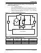
2.1 PFC BOOST CONVERTER
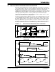
The conventional single-phase power factor correction circuit is a standard Boost
converter topology operating from the full wave rectified mains input, as shown in
Figure 2-1.
The converter controller has an inner current control loop and outer voltage control
loop. The current reference waveform is the input rectified mains voltage, so that the
resultant current drawn from the mains is essentially sinusoidal and in-phase with the
mains voltage. The amplitude of the current is controlled by the duty cycle of the fixed
frequency PWM of the MOSFET, and is controlled by the PWM reference, which is the
product of the current reference and the output of the DC link voltage error amplifier.
Refer to Chapter 1. “Introduction” for details on the operation of this converter.
FIGURE 2-1: PFC POWER CONVERTER
EQUATION 2-1:
EQUATION 2-2:
VDC
VAC
()
(
)
1
ac
dc
Vt
Dt
V
=−
22
1
1
100
ac
I
I
THD
I
−
=
%%
%