
User`s guide


SMPS AC/DC Reference Design User’s Guide
DS70320B-page 22 © 2008 Microchip Technology Inc.
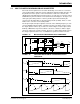
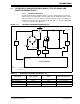
1.4.2 Phase-Shift ZVT Converter
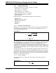
As indicated in the block diagram in Figure 1-19, three input signals are required to
implement the control algorithm. The only outputs from the dsPIC DSC device are firing
pulses to the Full-Bridge Phase-Shift ZVT and synchronous MOSFETs to control the
nominal voltage on V
OUT.
FIGURE 1-19: RESOURCES REQUIRED FOR DIGITAL PHASE-SHIFT ZVT CONVERTER
Table 1-2 shows the dsPIC DSC resources used by Phase-Shift ZVT application.
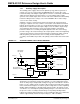
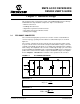
TABLE 1-2: RESOURCES REQUIRED FOR DIGITAL PHASE-SHIFT ZVT
k
4
k
5
dsPIC33FJ16GS504
ADC
Channel
ADC
Channel
UART
TX
PWM
UART
RX
PWM
PWM
IZVT
VHV_BUS
VOUT
Isolation
Barrier
ADC
Channel
PWM
PWM
PWM
FET
Driver
FET
Driver
FET
Driver
dsPIC33FJ16GS504
Note 1: K
4
and K
5
are feedback gain circuits. See A.3 “SMPS AC/DC Reference Design Schematics” for detailed
schematics.
(1)
(1)
Description Type of Signal
dsPIC
®
DSC
Resources Used
Expected Signal Level
ZVT C
URRENT 1 (IZVT1) Analog AN0 1.5V (maximum)
ZVT CURRENT 2 (IZVT2) Analog AN2 1.5V (maximum)
Voltage Sense (VOUT) Analog AN5 (secondary side) 2.79V (maximum)
ZVT Gate Drive Full-Bridge Drive Outputs,
Digital
PWM1H, PWM1L,
PWM2H, PWM2L
—
Synchronous Rectifier
Gate Drive
Sync FET Drive Outputs, Digital PWM3H, PWM3L —