
User`s guide


Introduction
© 2008 Microchip Technology Inc. DS70320B-page 21
1.4 LISTING OF I/O SIGNALS FOR EACH BLOCK, TYPE OF SIGNAL AND
EXPECTED SIGNAL LEVELS
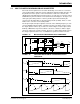
1.4.1 PFC Boost Converter
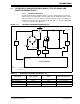
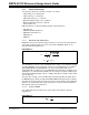
As indicated in the block diagram in Figure 1-18, three input signals are required to
implement the control algorithm. The only output from the dsPIC DSC device is firing
pulses to the Boost converter switch to control the nominal voltage on the DC bus in
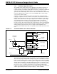
addition to presenting a resistive load to the AC line. Table 1-1 shows the dsPIC DSC
resources used by the PFC application.
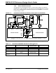
FIGURE 1-18: RESOURCES REQUIRED FOR DIGITAL PFC
TABLE 1-1: RESOURCES REQUIRED FOR DIGITAL PFC
Description Type of Signal
dsPIC
®
DSC Resources
Used
Expected Signal Level
Output Voltage (V
HV_BUS) Analog AN5 3.01V (nominal)
PFC Current (I
PFC) Analog AN4 2.5V (maximum)
AC Input Voltage (V
AC) Analog AN3 1.9V (maximum)
PFC Gate Drive PFC Drive Output, Digital PWM4L —
VAC
IPFC
VHV_BUS
ADC Channel
ADC Channel
ADC Channel
PWM Output
|V
AC|
k
1
k
2
k
3
FET Driver
dsPIC33FJ16GS504
(1)
(1)
(1)
Note 1: K
1
, K
2
and K
3
are feedback gain circuits. See A.3 “SMPS AC/DC Reference Design Schematics” for detailed
schematics.