
User`s guide


SMPS AC/DC Reference Design User’s Guide
DS70320B-page 20 © 2008 Microchip Technology Inc.
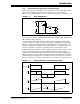
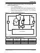
1.3.1 Auxiliary Supply Description
The auxiliary power supply is based on the flyback topology, where it generates a
voltage source for the control circuitry and MOSFET drivers on both sides of the
isolation boundary. The multiple output flyback converter is controlled by a TNY277G
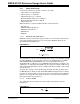
switch; the block diagram is shown in Figure 1-17. The auxiliary power supply
generates four isolated outputs, where on each side of the isolation barrier, the auxiliary
transformer will generate a voltage source for the MOSFET drivers and a voltage
source for the control circuitry.
A flyback converter is a transformer-isolated converter based on the basic Buck
topology. In a flyback converter, a switch is connected in series with the transformer
primary. The transformer is used to store energy during the ON period of the switch,
and provides isolation between the input voltage source V
IN and the output voltage
V
OUT. During the TOFF period, the energy stored in the primary of the flyback
transformer transfers to secondary through the flyback action. This stored energy
provides energy to the load, and charges the output capacitor. Since the magnetizing
current in the transformer cannot change instantaneously when the switch is turned
OFF, the primary current transfers to the secondary, and the amplitude of the
secondary current will be the product of the primary current and the transformer turns
ratio.
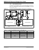
FIGURE 1-17: AUXILIARY POWER SUPPLY BLOCK DIAGRAM
At the end of the ON period, when the switch is turned OFF, there is no current path to
dissipate the stored leakage energy in the magnetic core of the flyback transformer.
There are many ways to dissipate this leakage energy. One such method is shown in
Figure 1-17 as a snubber circuit consisting of D, R, and C. In this method, the leakage
flux stored inside the magnetic core induces positive voltage at the non-dot end primary
winding, which forward-biases diode D and provides the path to the leakage energy
stored in the core, and clamps the primary winding voltage to a safe value. Because of
the presence of the secondary reflected voltage on the primary winding and the
leakage stored energy in the transformer core, the maximum voltage stress VDS of the
switch is approximately 1.6 times the input voltage (i.e., 400•1.6 = 660V).
HV Bias Supply
TNY277
-H
V_BUS
+HV_BUS
D
S
F/B
Live Drive
Supply
LIVE_GND
LIVE_GND
Live Digital
Supply
+13V
+7V
Drive Supply
GND
GND
Digital Supply
+17V
+7V
High-Voltage
Bus (400V)
Energy Efficient
Bias Supplies
Switching Converter
C
D
R