
User`s guide


SMPS AC/DC Reference Design User’s Guide
DS70320B-page 18 © 2008 Microchip Technology Inc.
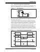
The inductor current is continuous and never reaches zero during one switching period
(T
S); therefore, this mode of operation is known as Continuous Conduction mode. In
Continuous Conduction mode, the relation between the output and input voltage is
given by Equation 1-1. The duty cycle is given by Equation 1-2.
EQUATION 1-1:
EQUATION 1-2:
When the output current requirement is high, the excessive power loss inside
freewheeling diode D1 limits the minimum output voltage that can be achieved. To
reduce the loss at high current, and to achieve lower output voltage, the freewheeling
diode is replaced by a MOSFET with a very low ON state resistance (R
DS(ON)). This
MOSFET is turned on and off synchronously with the Buck MOSFET. Therefore, this
topology is known as a Synchronous Buck converter. A gate drive signal, which is the
complement of the Buck switch gate drive signal, is required for this synchronous
MOSFET.
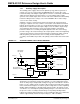
A MOSFET can conduct in either direction; which means the synchronous MOSFET
should be turned off immediately if the current in the inductor reaches zero because of
a light load. Otherwise, the direction of the inductor current will reverse (after reaching
zero) because of the output LC resonance. In such a scenario, the synchronous
MOSFET acts as a load to the output capacitor, and dissipates energy in the R
DS(ON)
of the MOSFET, resulting in an increase in power loss during the discontinuous mode
of operation (inductor current reaches zero in one switching cycle). This may happen if
the Buck converter inductor is designed for a medium load, but needs to operate at no
load and/or a light load. In this case, the output voltage may fall below the regulation
limit if the synchronous MOSFET is not switched off immediately after the inductor
reaches zero.
V
OUT
DV
IN
⋅=
where
D is the duty cycle
D
t
on
T
S
------
=
where t
on
is the ON time and T
S
is the switching time period