
User`s guide


Introduction
© 2008 Microchip Technology Inc. DS70320B-page 17
1.2.3 Buck Converter Description and Background
A Buck converter, as its name implies, can only produce lower average output voltage
than the input voltage. The basic schematic of a Buck converter is shown in
Figure 1-13. The switching waveforms for a Buck converter are shown in Figure 1-14.
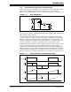
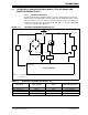
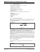
FIGURE 1-13: BUCK CONVERTER
In a Buck converter, a switch (Q1) is placed in series with the input voltage source V
IN.
Input source V
IN feeds the output through the switch and a low-pass filter, implemented
with an inductor and a capacitor.
In a steady state of operation, when the switch is ON for a period of T
ON, the input
provides energy to the output as well as to the inductor (L). During the T
ON period, the
inductor current flows through the switch and the difference of voltages between V
IN
and V
OUT is applied to the inductor in the forward direction, as shown in Figure 1-13.
Therefore, the inductor current I
L rises linearly from its present value IL1 to IL2.
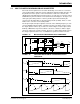
During the T
OFF period, when the switch is OFF, the inductor current continues to flow
in the same direction as the stored energy within the inductor, which continues to
supply the load current. Diode D1 completes the inductor current path during the Q1
OFF period (T
OFF); thus, it is called a freewheeling diode. During the TOFF period, the
output voltage V
OUT is applied across the inductor in the reverse direction, as shown in
Figure 1-14. Therefore, the inductor current decreases from its present value I
L2 to IL1.
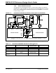
FIGURE 1-14: BUCK CONVERTER SWITCHING WAVEFORM
V
OUT
Q
1
D
1
I
IN
L
+
-
IL
I
OUT
V
IN
Q
1GATE
V
L
V
IN
- V
OUT
-V
OUT
-V
OUT
/L
I
IN
I
L
(V
IN
- V
OUT
)/L
t
t
t
t
I
L1
I
L2