
User`s guide

SMPS AC/DC Reference Design User’s Guide
DS70320B-page 16 © 2008 Microchip Technology Inc.
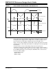
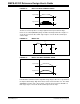
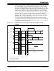
1.2.2.1 TIME INTERVALS
• Interval1: t0 < t < t1
Switch Q3 is turned OFF, beginning the resonant transition of the right leg. Pri-
mary current is maintained constant by the resonant inductor L
LK. The primary
current charges the output capacitor of switch Q3 (C
OSS3) to the input voltage
V
IN, which results in the output capacitance of Q4 (COSS4) being discharged to
zero potential. This creates zero potential across switch Q4 prior to turn-on, result-
ing in zero voltage switching. During this transition period, the transformer primary
voltage decreases from V
IN to zero, and the primary no longer supplies power to
the output. Inductive energy stored in the output inductor, and zero voltage across
the primary, cause both output MOSFETs to share the load current equally.
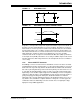
• Interval2: t1 < t < t2
After charging C
OSS3 to VIN, the primary current starts flowing through the body
diode of Q4. Q4 can then be turned on any time after t1 and have a zero voltage
turn-on transition.
• Interval3: t2 < t < t3
At t = t2, Q1 was turned OFF and the primary was maintained by the resonant
inductor L
LK. In addition, at t = t2, IP is slightly less than the primary peak current
I
PK because of finite losses. The primary resonant current charges the output
capacitor of switch Q1 (C
OSS1) to input voltage VIN, which discharges the output
capacitor of Q2 (C
OSS2) to zero potential, thus preparing for zero voltage turn-on
for switch Q2. During this transition, the primary current decays to zero. ZVS of
the left leg switches depending on the energy stored in the resonant inductor,
conduction losses in the primary switches and the losses in the transformer
winding. Since the left leg transition depends on leakage energy stored in the
transformer, it may require an external series inductor if the stored leakage energy
is not enough for ZVS. When Q2 is then turned ON in the next interval, voltage V
IN
is applied across the primary in the reverse direction.
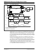
• Interval: t3 < t < t4
The two diagonal switches Q4, Q2 are ON, applying full input voltage across the
primary. During this period, the magnetizing current, plus the reflected secondary
current into the primary, flows through the switch. The exact diagonal switch-on
time depends on the input voltage, the transformer turns ratio and the output
voltage. After the switch-on time period of the diagonal switch, Q4 is turned OFF.
One switching cycle is completed when the switch Q4 is turned OFF. The primary
current charges C
OSS4 to a potential of input voltage VIN, and discharges COSS3
to zero potential, thereby enabling ZVS for switch Q3. The identical analysis is
required for the next half cycle.
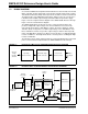
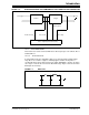
In the Phase-Shift ZVT converter shown in Figure 1-11, the maximum transition time
occurs for the left leg at minimum load current and maximum input voltage, and
minimum transition time occurs for the right leg at maximum load current and minimum
input voltage. Therefore, to achieve ZVT for all switches, enough inductive energy must
be stored to charge and discharge the output capacitance of the MOSFET in the
specified allocated time. Energy stored in the inductor must be greater than the
capacitive energy required for the transition. The MOSFET output capacitance varies
as applied drain-to-source voltage varies. Thus, the output capacitance of the
MOSFET should be multiplied by a factor of 4/3 to calculate the equivalent output
capacitance.