
User`s guide


SMPS AC/DC Reference Design User’s Guide
DS70320B-page 14 © 2008 Microchip Technology Inc.
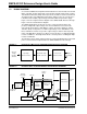
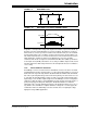
FIGURE 1-11: FULL-BRIDGE CONVERTER
In the Full-Bridge converter, four switches are used, thereby increasing the amount of
switching device loss. The conduction loss of a MOSFET can be reduced by using a
MOSFET with a low R
DS(ON) rating. Switching losses can be reduced by using Zero
Voltage Transition (ZVT), Zero Current Switching (ZCS), or both techniques. At high
power output and high input voltage, the ZVT technique is preferred for the MOSFET.
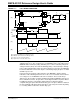
In a Phase-Shift ZVT converter, the output is controlled by varying the phase of switch
Q4 with respect to Q1.
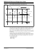
In this topology, the parasitic output capacitor of the MOSFETs, and the leakage
inductance of the switching transformer, are used as a resonant tank circuit to achieve
zero voltage across the MOSFET at the turn-on transition. There are two major
differences in the operation of a Phase-Shift ZVT and simple Full-Bridge topology. In a
Phase-Shift ZVT converter, the gate drive of both diagonal switches is phase shifted.
In addition, both halves of the bridge switch network are driven through the
complementary gate pulse with a fixed 50% duty cycle. The phase difference between
the two half-bridge switching network gate drives control the power flow from primary
to secondary, which results in the effective duty cycle.
V
IN
D
3
+
-
D
4
Q
4
Q
3
L
+
V
L
Q
1PWM
Q
3PWM
V
IN
Q
1
Q
2
V
IN
Q
4PWM
Q
2PWM
C
OSS1
C
OSS2
C
OSS3
C
OSS4
L
LKG
(A) = Full-Bridge/Half-Bridge Phase-Shift ZVT converter
(B) = PWM gate pulse waveform for Full-Bridge switches
(C) = Voltage across the transformer primary
(D) = Output inductor and rectifier diode current
(A)
(B)
(C)
(D)
-
C
O
V
OUT
T
ON
T
OFF
T
S