
User`s guide

Introduction
© 2008 Microchip Technology Inc. DS70320B-page 13
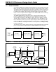
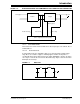
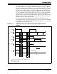
FIGURE 1-9: BUCK/BOOST PFC
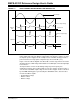
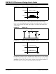
FIGURE 1-10: BUCK/BOOST PFC INPUT CURRENT SHAPE
Regardless of the input line voltage and output load variations, input current drawn by
the Buck converter and the Buck/Boost converter is always discontinuous. However,
when the Boost converter operates in Continuous Conduction mode, the current drawn
from the input voltage source is always continuous and smooth as shown in Figure 1-8.
This feature makes the Boost converter an ideal choice for the Power Factor Correction
(PFC) application. In PFC, the input current drawn by the converter should be
continuous and smooth enough to meet Total Harmonic Distortion (THD) specifications
for the input current (ITHD) such that it is close to unity. In addition, input current should
follow the input sinusoidal voltage waveform to meet displacement factor such that it is
close to unity.
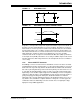
1.2.2 Phase-Shift ZVT Converter
A Full-Bridge converter is a transformer isolated Buck converter. The basic schematic
and switching waveform is shown in Figure 1-11. The transformer primary is connected
between the two legs formed by switches Q1,Q2 and Q4,Q3. Switches Q1,Q2 and Q4,
Q3 create a pulsating AC voltage at the transformer primary. The transformer is used
to step down the pulsating primary voltage, as well as to provide isolation between the
input voltage source and the output voltage V
OUT. A Full-Bridge converter configuration
retains the voltage properties of the Half-Bridge topology, and the current properties of
push-pull topology. The diagonal switch pairs, Q1,Q3 and Q4,Q2, are switched
alternately at the selected switching period. Since the maximum voltage stress across
any switch is V
IN, and with the complete utilization of magnetic core and copper, this
combination makes the Full-Bridge converter an ideal choice for high input voltage,
high-power range SMPS applications.
+
Co
D
-
L
Input Current
Input Voltage
t
t