
User`s guide

SMPS AC/DC Reference Design User’s Guide
DS70320B-page 12 © 2008 Microchip Technology Inc.
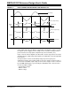
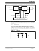
FIGURE 1-6: BUCK PFC INPUT CURRENT SHAPE
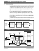
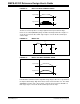
1.2.1.2.2 Boost PFC Circuit
The Boost converter produces a voltage higher than the input rectified voltage;
therefore, the switch (MOSFET) rating should be rated higher than V
OUT. Figure 1-7
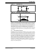
shows the circuit for the Boost PFC stage. Figure 1-8 shows the Boost PFC input
current shape.
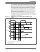
FIGURE 1-7: BOOST PFC
FIGURE 1-8: BOOST PFC INPUT CURRENT SHAPE
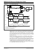
1.2.1.2.3 Buck/Boost PFC Circuit
In the Buck/Boost PFC circuit, the output DC voltage may be either less or greater than
the input rectified voltage. High Power Factor can be achieved in this case. The switch
(MOSFET) is rated to (V
IN + VOUT). Figure 1-9 shows the circuit for the Buck/Boost
PFC stage. Figure 1-10 shows the Boost PFC input current shape.
Input Current
Input Voltage
t
t
+
Co
D
-
L
Input Current
Input Voltage
t
t