
User`s guide

Introduction
© 2008 Microchip Technology Inc. DS70320B-page 11
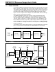
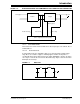
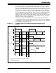
FIGURE 1-4: BLOCK DIAGRAM OF THE COMPONENTS FOR POWER FACTOR CORRECTION
1.2.1.2 PFC TOPOLOGIES
The Power Factor can be achieved with various basic topologies such as Buck, Boost
and Buck/Boost.
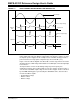
1.2.1.2.1 Buck PFC Circuit
In a Buck PFC circuit, the output DC voltage is less than the input rectified voltage.
Large filters are needed to suppress switching ripples and this circuit produces
considerable Power Factor improvement. The switch (MOSFET) is rated to V
IN in this
case. Figure 1-5 shows the circuit for the Buck PFC stage. Figure 1-6 shows the Buck
PFC input current shape.
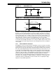
FIGURE 1-5: BUCK PFC
Rectifier Chopper
Rectified Voltage
Bus Current
DC Voltage
dsPIC
®
Digital Signal Controller (DSC)
Load
AC Input
Switching pulses
+
Co
-
D
L