
User`s guide

SMPS AC/DC Reference Design User’s Guide
DS70320B-page 8 © 2008 Microchip Technology Inc.
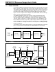
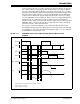
1.2 BLOCK DIAGRAM
A conventional SMPS must implement PFC if it draws more than 75 watts from the AC
Mains. The PFC circuitry draws input current in phase with the input voltage, and the
Total Harmonic Distortion (THD) of the input current should be less than 5% at full load.
The PFC provides a fixed DC high-output voltage, which needs to be converted to a
lower Direct Current (DC) output voltage and isolated with an input mains supply.
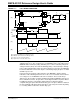
Figure 1-2 shows a high-level block diagram of the SMPS AC/DC Reference Design.
Figure 1-2 shows a detailed block diagram.
The SMPS AC/DC Reference Design operates on universal input voltage and
produces multiple DC output voltages. The front-end PFC Boost circuit converts
universal AC input voltage to 420 VDC bus voltage. The Phase-Shift Zero Voltage
Transition (ZVT) circuit produces 12 VDC output voltage from a 420 VDC bus. The
Phase-Shift ZVT converter also provides output voltage isolation from the input AC
mains. The Multi-Phase Synchronous Buck converter produces 3.3 VDC @ 69 Amps
from the 12 VDC bus. The Single-Phase Buck converter produces 5 VDC @ 23 Amps
from the 12 VDC bus.
The following sections in this chapter provide an overview and background of the main
power conversion blocks implemented in the SMPS AC/DC Reference Design.
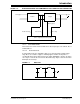
FIGURE 1-1: HIGH-LEVEL SMPS AC/DC REFERENCE DESIGN BLOCK DIAGRAM
FIGURE 1-2: DETAILED SMPS AC/DC REFERENCE DESIGN BLOCK DIAGRAM
Input Stage
AC-DC Converter
Intermediate Stage
DC-DC Converter
Point of Load
DC-DC Converter
AC Input
Voltage
85-265V
45-65 Hz
Multiple
DC Outputs
85-265 VAC
45-65 Hz
EMI Filter
and Bridge
Rectifier
PFC
Boost
Converter
ZVT
Full-Bridge
Converter
Synchronous
Rectifier
Optocoupler
3.3 VDC
69A
5 V
DC
23A
Isolation
Barrier
420 V
DC
Rectified
Sinusoidal
Voltage
Multi-Phase
Buck Converter
Single-Phase
Buck Converter
Phase-Shift ZVT Converter
dsPIC33FJ16GS504
dsPIC33FJ16GS504
12 VDC
30A