
User`s guide

SMPS AC/DC REFERENCE
DESIGN USER’S GUIDE
© 2008 Microchip Technology Inc. DS70320B-page 7
Chapter 1. Introduction
This chapter provides an introduction to the SMPS AC/DC Reference Design and
includes the following major topics:
• System Specifications
•Block Diagram
• Multi-Phase Synchronous Buck Converter
• Listing of I/O Signals for Each Block, Type of Signal and Expected Signal Levels
1.1 SYSTEM SPECIFICATIONS
This reference design describes the design of an off-line Switch Mode Power Supply
(SMPS) design using an SMPS dsPIC
®
DSC (dsPIC33FJ16GS504).
The SMPS AC/DC Reference Design works with universal input voltage range and
produces three output voltages (12V, 3.3V and 5V). The continuous output rating of the
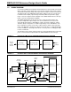
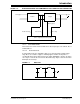
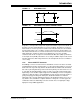
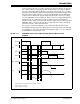
reference design is 300 Watts. This reference design is based on a modular structure
having three major block sets as shown in Figure 1-1. Figure 1-2 shows a more
detailed block diagram with all functional blocks as implemented on the SMPS AC/DC
Reference Design.
The Power Factor Circuit (PFC) converts the universal AC input voltage to constant
high-voltage DC, and maintains the sinusoidal input current at high power factor. The
Phase-Shift Zero Voltage Transition circuit converts high-voltage DC to intermediate
low-voltage DC with isolation from the input AC mains, at high efficiency. The
Multi-Phase Synchronous and Single-Phase Synchronous Buck circuit converts
intermediate low-voltage DC to very low-voltage DC at high current at high efficiency.
The input and output specifications are as follows:
• Input:
- Input voltage: 85 V
AC-265 VAC
- Input frequency: 45 Hz-65 Hz
• Outputs (individually loaded):
- Output voltage 1 (Vo 1 ) = 12V
- Output load 1 (Io1) = 0A-30A
- Output voltage 2 (Vo 2 ) = 3.3V
- Output load 2 (Io2) = 0A-69A
- Output voltage 3 (Vo 3 ) = 5V
- Output load 3 (Io3) = 0A-23A
• Outputs (simultaneously loaded):
- Output voltage 2 (Vo 2 ) = 3.3V
- Output load 2 (Io2) = 0A-56A
- Output voltage 3 (Vo 3 ) = 5V
- Output load 3 (Io3) = 0A-23A