
Service Manual

9LWHOFRP0REL O H7HFKQRORJ\6$ 3URSULHWDU\DQG&RQILGHQWLDO - 19 -
V
V
I
I
T
T
E
E
L
L
C
C
O
O
M
M
M
M
O
O
B
B
I
I
L
L
E
E
T
T
E
E
C
C
H
H
N
N
O
O
L
L
O
O
G
G
Y
Y
S
S
.
.
A
A
.
.
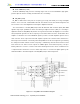
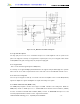
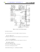
Figure 4.8 VTL501 Logic Part Block Diagram
4.4 Power Up Sequence
This section describes the steps how the TSM501 / VTL501 phone wakes up.
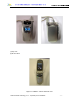
Place a Battery Pack
The battery pack, which the protection circuit is implemented, is placed into the phone.
Press and Hold [END] Key
The Power on circuit (SW124) generates the control voltage to be used for U6.
Regulators Activated
U6 feeds 2.8V to MSM (U125), LCD
U6 feeds 2.8V to Flash ROM / SRAM (U113) and others.
U6 feeds 2.8V to VCTCXO(U104) and others.