
Technical data

18
Chapter 1: DVP Specifications
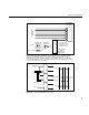
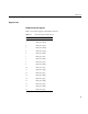
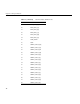
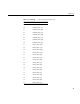
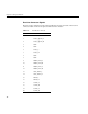
Receiver Connector Signals
Because of the construction of the external cable, the pinout is reversed on the receiver
connector. Table 1-2 shows the pinout of the receiver connector.
Table 1-2 DVP Receiver Pinouts
Pin No. Pin Name
MTG1 CHASSIS_GND
1 CLK_2_QUAD_L
2 CLK_2_QUAD_H
3 GND
4 GND
5 CLK_2_L
6 CLK_2_H
7 GND
8 GND
9 HMUX_SEL0_L
10 HMUX_SEL0_H
11 HMUX_SEL1_L
12 HMUX_SEL1_H
13 VOC_SWAP_L
14 VOC_SWAP_H
15 FIELD_L
16 FIELD_H
17 VSYNC_L
18 VSYNC_H
19 CSYNC_L
20 CSYNC_H