
Technical data

Electrical Considerations
9
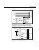
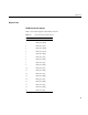
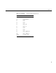
Figure 1-4 Recommended Receiver Design
DQ
*Q
DQ
*Q
Clock/2
Clock/2_quad
ELC Shft
(clk/2)
SY100EL07
140/415 psec
1:9 Differential
clock driver
MC100E111
430/630 psec
SY100EL16
175/355 psec
Clock/2
Clock/2_quad
SY100EL16A
175/355 psec
Note: allow 200psec (1.12 in.) each for the wires between the EL16A and the EL07, and for
the wires between the EL07 and the E111. Allow 750psec (4.2 in.) for the wires from the
100E111 to the 100E452 registers’ clock inputs, to get the total delay of this scheme:
1895/2550 psec. In order to meet the hold time of the 100E452, make sure the data lines
are 1.62 inches (300psec) longer to the differential data inputs of the E452 than the length of
CLK/2 and CLK/2_QUAD to the EL16A’s.
MC100E452
ts = 150psec
th = 250psec
On DVP1 Board:
DVP Differential
Data (typ)
Keep all clock
line lengths equal
from E111 to all
receiving registers.
Recovered clock
DQ
*Q
Data
Data_pre
Clock
On Receiver Board: