
Datasheet
VS-MBR4045CTPbF, VS-MBR4045CT-N3
www.vishay.com
Vishay Semiconductors
Revision: 30-Aug-11
2
Document Number: 94294
For technical questions within your region: DiodesAmericas@vishay.com
, DiodesAsia@vishay.com, DiodesEurope@vishay.com
THIS DOCUMENT IS SUBJECT TO CHANGE WITHOUT NOTICE. THE PRODUCTS DESCRIBED HEREIN AND THIS DOCUMENT
ARE SUBJECT TO SPECIFIC DISCLAIMERS, SET FORTH AT www.vishay.com/doc?91000
Note
(1)
Pulse width < 300 μs, duty cycle < 2 %
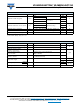
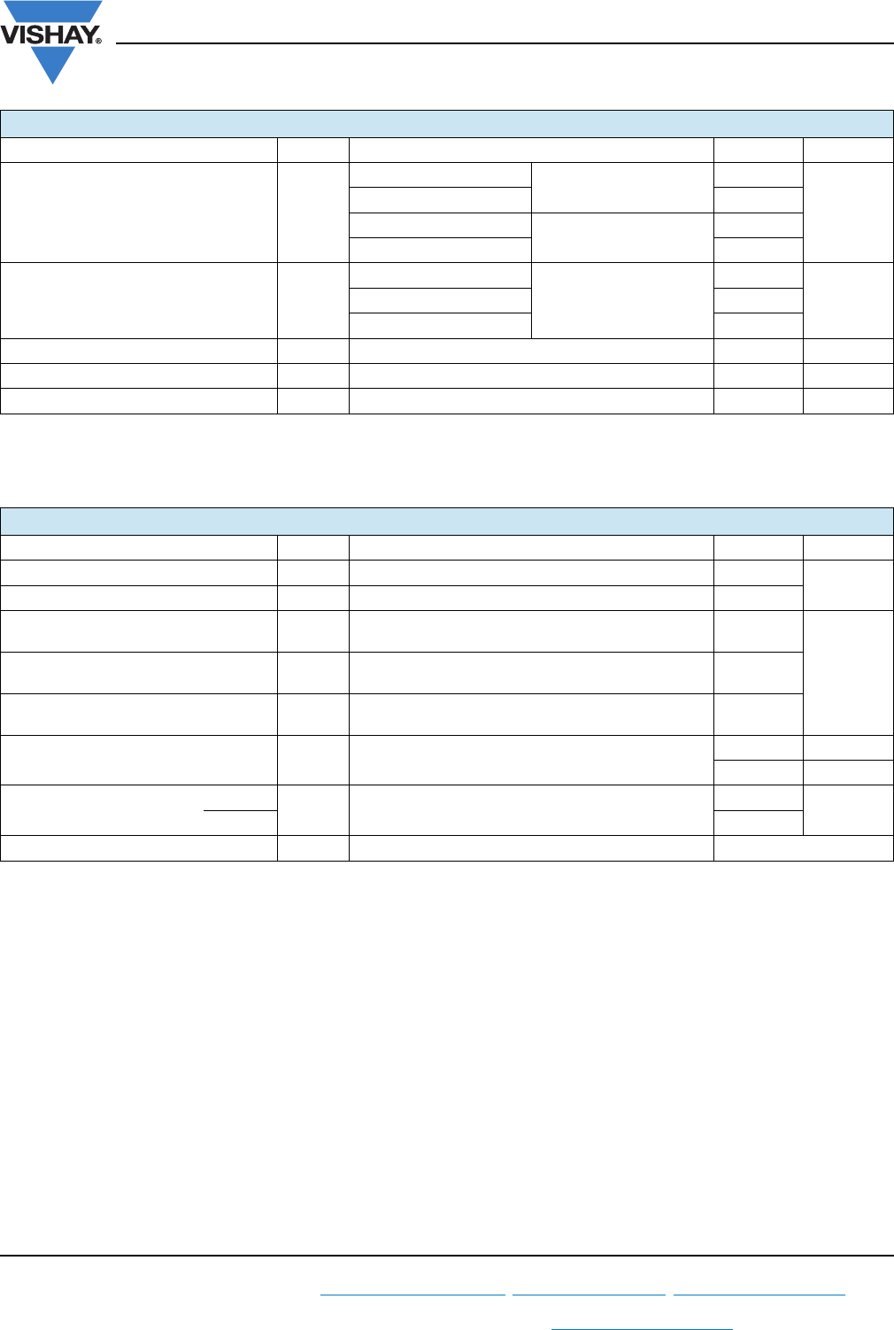
ELECTRICAL SPECIFICATIONS
PARAMETER SYMBOL TEST CONDITIONS VALUES UNITS
Maximum forward voltage drop V
FM
(1)
20 A
T
J
= 25 °C
0.60
V
40 A 0.78
20 A
T
J
= 125 °C
0.58
40 A 0.75
Maximum instantaneus reverse current I
RM
(1)
T
J
= 25 °C
Rated DC voltage
1
mAT
J
= 100 °C 50
T
J
= 125 °C 95
Maximum junction capacitance C
T
V
R
= 5 V
DC,
(test signal range 100 kHz to 1 MHz) 25 °C 900 pF
Typical series inductance L
S
Measured from top of terminal to mounting plane 8.0 nH
Maximum voltage rate of change dV/dt Rated V
R
10 000 V/µs
THERMAL - MECHANICAL SPECIFICATIONS
PARAMETER SYMBOL TEST CONDITIONS VALUES UNITS
Maximum junction temperature range T
J
- 65 to 150
°C
Maximum storage temperature range T
Stg
- 65 to 175
Maximum thermal resistance,
junction to case per leg
R
thJC
DC operation 1.5
°C/W
Typical thermal resistance,
case to heatsink
R
thCS
Mounting surface, smooth and greased
(Only for TO-220)
0.50
Maximum thermal resistance,
junction to ambient
R
thJA
DC operation
(For D
2
PAK and TO-262)
50
Approximate weight
2g
0.07 oz.
Mounting torque
minimum
Non-lubricated threads
6 (5)
kgf · cm
(lbf · in)
maximum 12 (10)
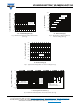
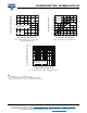
Marking device Case style TO-220AB MBR4045CT