
Datasheet

VS-HFA04SD60SPbF
www.vishay.com
Vishay Semiconductors
Revision: 14-Jun-11
2
Document Number: 94034
For technical questions within your region: DiodesAmericas@vishay.com
, DiodesAsia@vishay.com, DiodesEurope@vishay.com
THIS DOCUMENT IS SUBJECT TO CHANGE WITHOUT NOTICE. THE PRODUCTS DESCRIBED HEREIN AND THIS DOCUMENT
ARE SUBJECT TO SPECIFIC DISCLAIMERS, SET FORTH AT www.vishay.com/doc?91000
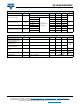
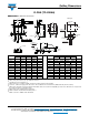
DYNAMIC RECOVERY CHARACTERISTICS (T
C
= 25 °C unless otherwise specified)
PARAMETER SYMBOL TEST CONDITIONS MIN. TYP. MAX. UNITS
Reverse recovery time t
rr
I
F
= 1.0 A, dI
F
/dt = 200 A/μA, V
R
= 30 V - 17 -
nsT
J
= 25 °C
I
F
= 4 A
dI
F
/dt = 200 A/μs
V
R
= 200 V
-2842
T
J
= 125 °C - 38 57
Peak recovery current I
RRM
T
J
= 25 °C - 2.9 5.2
A
T
J
= 125 °C - 3.7 6.7
Reverse recovery charge Q
rr
T
J
= 25 °C - 40 60
nC
T
J
= 125 °C - 70 105
Rate of fall of recovery current dI
(rec)M
/dt
T
J
= 25 °C - 280 -
A/μs
T
J
= 125 °C - 235 -
THERMAL - MECHANICAL SPECIFICATIONS
PARAMETER SYMBOL TEST CONDITIONS MIN. TYP. MAX. UNITS
Maximum junction and
storage temperature range
T
J
, T
Stg
- 55 - 150 °C
Thermal resistance,
junction to case
R
thJC
--5.0
°C/W
Thermal resistance,
junction to ambient
R
thJA
Typical socket mount - - 80
Weight
-2.0- g
-0.07- oz.
Mounting torque
6.0
(5.0)
-
12
(10)
kgf · cm
(lbf in)
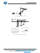
Marking device Case style D-PAK HFA04SD60S