
Datasheet

VS-ETL0806-M3, VS-ETL0806FP-M3
www.vishay.com
Vishay Semiconductors
Revision: 16-Apr-14
5
Document Number: 93528
For technical questions within your region: DiodesAmericas@vishay.com
, DiodesAsia@vishay.com, DiodesEurope@vishay.com
THIS DOCUMENT IS SUBJECT TO CHANGE WITHOUT NOTICE. THE PRODUCTS DESCRIBED HEREIN AND THIS DOCUMENT
ARE SUBJECT TO SPECIFIC DISCLAIMERS, SET FORTH AT www.vishay.com/doc?91000
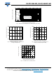
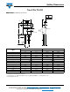
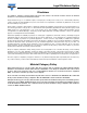
Fig. 9 - Typical Reverse Recovery vs. dI
F
/dt Fig. 10 - Typical Stored Charge vs. dI
F
/dt
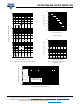
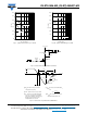
Fig. 11 - Reverse Recovery Parameter Test Circuit
Fig. 12 - Reverse Recovery Waveform and Definitions
trr ( ns )
di
F
/dt (A/µs )
100 1000
80
120
160
200
240
280
320
360
If = 8A, 125°C
If = 8A, 25°C
typical value
Qrr ( nC )
di
F
/dt (A/µs )
100 1000
0
500
1000
1500
2000
2500
3000
3500
If = 8A, 125°C
If = 8A, 25°C
typical value
IRFP250
D.U.T.
L = 70 μH
V
R
= 200 V
0.01 Ω
G
D
S
dI
F
/dt
adjust
Q
rr
0.5 I
RRM
dI
(rec)M
/dt
0.75 I
RRM
I
RRM
t
rr
t
b
t
a
I
F
dI
F
/dt
0
(1)
(2)
(3)
(4)
(5)
(1) dI
F
/dt - rate of change of current
through zero crossing
(2) I
RRM
- peak reverse recovery current
(3) t
rr
- reverse recovery time measured
from zero crossing point of negative
going I
F
to point where a line passing
through 0.75 I
RRM
and 0.50 I
RRM
extrapolated to zero current.
(4) Q
rr
- area under curve dened by t
rr
and I
RRM
t
rr
x I
RRM
2
Q
rr
=
(5) dI
(rec)M
/dt - peak rate of change of
current during t
b
portion of t
rr