
Datasheet


VS-APU3006-F3, VS-APU3006-N3, VS-EPU3006-F3, VS-EPU3006-N3
www.vishay.com
Vishay Semiconductors
Revision: 28-Mar-14
4
Document Number: 93570
For technical questions within your region: DiodesAmericas@vishay.com
, DiodesAsia@vishay.com, DiodesEurope@vishay.com
THIS DOCUMENT IS SUBJECT TO CHANGE WITHOUT NOTICE. THE PRODUCTS DESCRIBED HEREIN AND THIS DOCUMENT
ARE SUBJECT TO SPECIFIC DISCLAIMERS, SET FORTH AT www.vishay.com/doc?91000
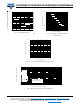
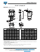
Fig. 5 - Maximum Allowable Case Temperature vs.
Average Forward Current
Fig. 6 - Forward Power Loss Characteristics
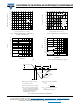
Fig. 7 - Typical Reverse Recovery Time vs. dI
F
/dt Fig. 8 - Typical Stored Charge vs. dI
F
/dt
Fig. 9 - Reverse Recovery Waveform and Definitions
Average Forward Current - I
F(AV)
(A)
0 5 10 15 20 25 30 35 40 45
100
110
120
130
140
150
160
170
180
DC
Allowable Case Temperature (°C)
Average Forward Current - IF
(AV)
(V)
Average Power Loss (W)
0 5 10 15 20 25 30 35 40 45
0
10
20
30
40
50
60
D = 0.01
D = 0.02
D = 0.05
D = 0.1
D = 0.2
D = 0.5
DC
RMS Limit
t
rr
(ns)
dI
F
/dt (A/μs)
100 1000
10
20
30
40
50
60
70
80
90
100
110
120
130
I
F
= 30 A, 125 °C
I
F
= 30 A, 25 °C
typical value
Q
rr
(nC)
dI
F
/dt (A/μs)
100 1000
0
200
400
600
800
1000
1200
1400
1600
1800
I
F
= 30 A, 125 °C
I
F
= 30 A, 25 °C
typical value
Q
rr
0.5 I
RRM
dI
(rec)M
/dt
0.75 I
RRM
I
RRM
t
rr
t
b
t
a
I
F
dI
F
/dt
0
(1)
(2)
(3)
(4)
(5)
(1) dI
F
/dt - rate of change of current
through zero crossing
(2) I
RRM
- peak reverse recovery current
(3) t
rr
- reverse recovery time measured
from zero crossing point of negative
going I
F
to point where a line passing
through 0.75 I
RRM
and 0.50 I
RRM
extrapolated to zero current.
(4) Q
rr
- area under curve dened by t
rr
and I
RRM
t
rr
x I
RRM
2
Q
rr
=
(5) dI
(rec)M
/dt - peak rate of change of
current during t
b
portion of t
rr