
Datasheet

VS-50WQ06FN-M3
www.vishay.com
Vishay Semiconductors
Revision: 22-Nov-16
2
Document Number: 93313
For technical questions within your region: DiodesAmericas@vishay.com
, DiodesAsia@vishay.com, DiodesEurope@vishay.com
THIS DOCUMENT IS SUBJECT TO CHANGE WITHOUT NOTICE. THE PRODUCTS DESCRIBED HEREIN AND THIS DOCUMENT
ARE SUBJECT TO SPECIFIC DISCLAIMERS, SET FORTH AT www.vishay.com/doc?91000
Note
(1)
Pulse width < 300 μs, duty cycle < 2 %
Note
(1)
thermal runaway condition for a diode on its own heatsink
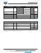
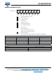
ELECTRICAL SPECIFICATIONS
PARAMETER SYMBOL TEST CONDITIONS VALUES UNITS
Maximum forward voltage drop
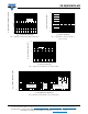
See fig. 1
V
FM
(1)
5 A
T
J
= 25 °C
0.57
V
10 A 0.74
5 A
T
J
= 125 °C
0.54
10 A 0.68
Maximum reverse leakage current
See fig. 2
I
RM
(1)
T
J
= 25 °C
V
R
= Rated V
R
3
mA
T
J
= 125 °C 35
Threshold voltage V
F(TO)
T
J
= T
J
maximum
0.35 V
Forward slope resistance r
t
25.5 m
Typical junction capacitance C
T
V
R
= 5 V
DC
(test signal range 100 kHz to 1 MHz), 25 °C 360 pF
Typical series inductance L
S
Measured lead to lead 5 mm from package body 5.0 nH
Maximum voltage rate of change dV/dt Rated V
R
10 000 V/μs
THERMAL - MECHANICAL SPECIFICATIONS
PARAMETER SYMBOL TEST CONDITIONS VALUES UNITS
Maximum junction and storage
temperature range
T
J
(1)
, T
Stg
-40 to +150 °C
Maximum thermal resistance,
junction to case
R
thJC
DC operation
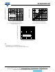
See fig. 4
3.0 °C/W
Approximate weight
0.3 g
0.01 oz.
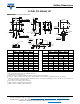
Marking device Case style D-PAK (similar to TO-252AA) 50WQ06FN
dP
tot
dT
J
-------------
1
R
thJA
--------------<