
Datasheet

Document Number: 95016 For technical questions concerning discrete products, contact: diodes-tech@vishay.com
www.vishay.com
Revision: 04-Nov-08 For technical questions concerning module products, contact: ind-modules@vishay.com
1
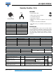
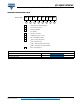
D-PAK (TO-252AA)
Outline Dimensions
Vishay High Power Products
Notes
(1)
Dimensioning and tolerancing as per ASME Y14.5M-1994
(2)
Lead dimension uncontrolled in L5
(3)
Dimension D1, E1, L3 and b3 establish a minimum mounting surface for thermal pad
(4)
Section C - C dimension apply to the flat section of the lead between 0.13 and 0.25 mm (0.005 and 0.10") from the lead tip
(5)
Dimension D, and E do not include mold flash. Mold flash shall not exceed 0.127 mm (0.005") per side. These dimensions are measured at
the outermost extremes of the plastic body
(6)
Dimension b1 and c1 applied to base metal only
(7)
Datum A and B to be determined at datum plane H
(8)
Outline conforms to JEDEC outline TO-252AA
DIMENSIONS in millimeters and inches
SYMBOL
MILLIMETERS INCHES
NOTES SYMBOL
MILLIMETERS INCHES
NOTES
MIN. MAX. MIN. MAX. MIN. MAX. MIN. MAX.
A 2.18 2.39 0.086 0.094 e 2.29 BSC 0.090 BSC
A1 - 0.13 - 0.005 H 9.40 10.41 0.370 0.410
b 0.64 0.89 0.025 0.035 L 1.40 1.78 0.055 0.070
b2 0.76 1.14 0.030 0.045 L1 2.74 BSC 0.108 REF.
b3 4.95 5.46 0.195 0.215 3 L2 0.51 BSC 0.020 BSC
c 0.46 0.61 0.018 0.024 L3 0.89 1.27 0.035 0.050 3
c2 0.46 0.89 0.018 0.035 L4 - 1.02 - 0.040
D 5.97 6.22 0.235 0.245 5 L5 1.14 1.52 0.045 0.060 2
D1 5.21 - 0.205 - 3 Ø 0° 10° 0° 10°
E 6.35 6.73 0.250 0.265 5 Ø1 0° 15° 0° 15°
E1 4.32 - 0.170 - 3 Ø2 25° 35° 25° 35°
Ø 1
E
(5)
b3
(3)
0.010
CAB
L3 (3)
B
A
C
H
C
L2
D (5)
L4
b
2 x
e
b2
(2) L5
1
2
3
4
Ø 2
A
c2
A
A
H
Seating
plane
c
Detail “C”
(7)
Seating
plane
A1
Detail “C”
Rotated 90 °CW
Scale: 20:1
(L1)
C
C
L
Ø
Gauge
plane
Lead tip
M
0.010
CAB
M
32
4
1
E1
D1
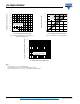
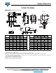
MIN.
0.265
(6.74)
MIN.
0.245
(6.23)
MIN.
0.089
(2.28)
MIN.
0.06
(1.524)
0.488 (12.40)
0.409 (10.40)
0.093 (2.38)
0.085 (2.18)
Pad layout