
Datasheet


Document Number: 95180 For technical questions within your region, please contact one of the following: www.vishay.com
Revision: 25-Oct-10 DiodesAmericas@vishay.com
, DiodesAsia@vishay.com, DiodesEurope@vishay.com 1
TO-220AB, TO-220AC
Outline Dimensions
Vishay Semiconductors
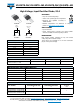
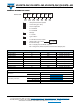
DIMENSIONS FOR TO-220AB in millimeters and inches
Notes
(1)
Dimensioning and tolerancing per ASME Y14.5M-1994
(2)
Lead dimension and finish uncontrolled in L1
(3)
Dimension D and E do not include mold flash. Mold flash shall not exceed 0.127 mm (0.005") per side. These dimensions are measured at
the outermost extremes of the plastic body
(4)
Dimension b1 and c1 apply to base metal only
(5)
Controlling dimensions: inches
SYMBOL
MILLIMETERS INCHES
NOTES SYMBOL
MILLIMETERS INCHES
NOTES
MIN. MAX. MIN. MAX. MIN. MAX. MIN. MAX.
A 4.25 4.65 0.167 0.183 D2 12.19 12.88 0.480 0.507
A1 1.14 1.40 0.045 0.055 E 10.11 10.51 0.398 0.414 3
A2 2.56 2.92 0.101 0.115 E1 8.38 8.89 0.330 0.350
b 0.69 1.01 0.027 0.040 e 2.41 2.67 0.095 0.105
b1 0.38 0.96 0.015 0.038 4 e1 4.88 5.28 0.192 0.208
b2 1.20 1.73 0.047 0.068 H1 6.09 6.48 0.240 0.255
b3 1.15 1.73 0.045 0.068 L 13.52 14.02 0.532 0.552
c 0.36 0.61 0.014 0.024 L1 3.32 3.82 0.131 0.150 2
c1 0.36 0.56 0.014 0.022 4 Ø P 3.54 3.73 0.139 0.147
c2 0.31 1.14 0.012 0.045 Q 2.60 3.00 0.102 0.118
D 14.85 15.25 0.585 0.600 3 90° to 93° 90° to 93°
D1 8.38 9.02 0.330 0.355
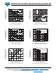
32
4
1
DD
CC
D
Q
D1
E
A
Ø P
(3)
Detail B
L1
(2)
L
C
e1
2 x e
0.015 ABC
MM
B
Seating plane
H1
A
A
A
A1
A2
C
Sheet 2
View A - A
θ
H1
E
D2
Thermal pad
E1
Detail B
3 x b2 3 x b
D
L1
D
123
C
C
b, b2
c1
b1, b3
Section C - C and D - D
c
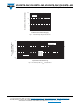
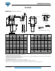
Lead assignments
HEXFET
1. - Gate
2. - Drain
3. - Source
IGBTs, CoPAK
1. - Gate
2. - Collector
3. - Emitter
Diodes
1. - Anode/open
2. - Cathode
3. - Anode