
Datasheet


VS-20ETF..SPbF Series
www.vishay.com
Vishay Semiconductors
Revision: 18-Dec-13
2
Document Number: 94097
For technical questions within your region: DiodesAmericas@vishay.com
, DiodesAsia@vishay.com, DiodesEurope@vishay.com
THIS DOCUMENT IS SUBJECT TO CHANGE WITHOUT NOTICE. THE PRODUCTS DESCRIBED HEREIN AND THIS DOCUMENT
ARE SUBJECT TO SPECIFIC DISCLAIMERS, SET FORTH AT www.vishay.com/doc?91000
Note
(1)
When mounted on 1" square (650 mm
2
) PCB of FR-4 or G-10 material 4 oz. (140 μm) copper 40 °C/W.
For recommended footprint and soldering techniques refer to application note #AN-994.
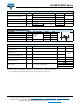
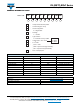
ELECTRICAL SPECIFICATIONS
PARAMETER SYMBOL TEST CONDITIONS VALUES UNITS
Maximum forward voltage drop V
FM
20 A, T
J
= 25 °C 1.30
V
60 A, T
J
= 25 °C 1.67
Forward slope resistance r
t
12.5 m
Threshold voltage V
F(TO)
T
J
= 150 °C 0.9 V
Maximum reverse leakage current I
RM
T
J
= 25 °C
V
R
= Rated V
RRM
0.1
mA
T
J
= 150 °C 5.0
RECOVERY CHARACTERISTICS
PARAMETER SYMBOL TEST CONDITIONS VALUES UNITS
Reverse recovery time t
rr
I
F
at 20 A
pk
100 A/μs
25 °C
160 ns
Reverse recovery current I
rr
10 A
Reverse recovery charge Q
rr
1.25 μC
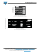
Snap factor S Typical 0.6
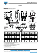
I
FM
t
rr
dir
dt
I
RM(REC)
Q
rr
t
t
a
t
b
THERMAL - MECHANICAL SPECIFICATIONS
PARAMETER SYMBOL TEST CONDITIONS VALUES UNITS
Maximum junction and storage
temperature range
T
J
, T
Stg
-40 to 150 °C
Maximum thermal resistance,
junction to case
R
thJC
DC operation 0.9
°C/W
Maximum thermal resistance
junction to ambient (PCB mount)
R
thJA
(1)
40
Soldering temperature T
S
260 °C
Approximate weight
2g
0.07 oz.
Marking device Case style TO-263AB (D
2
PAK)
20ETF02S
20ETF04S
20ETF06S