
Datasheet


VS-20ETF0...PbF Series, VS-20ETF0...-M3 Series
www.vishay.com
Vishay Semiconductors
Revision: 26-Jul-13
2
Document Number: 94096
For technical questions within your region: DiodesAmericas@vishay.com
, DiodesAsia@vishay.com, DiodesEurope@vishay.com
THIS DOCUMENT IS SUBJECT TO CHANGE WITHOUT NOTICE. THE PRODUCTS DESCRIBED HEREIN AND THIS DOCUMENT
ARE SUBJECT TO SPECIFIC DISCLAIMERS, SET FORTH AT www.vishay.com/doc?91000
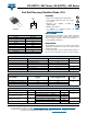
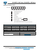
ELECTRICAL SPECIFICATIONS
PARAMETER SYMBOL TEST CONDITIONS VALUES UNITS
Maximum forward voltage drop V
FM
20 A, T
J
= 25 °C 1.3 V
Forward slope resistance r
t
T
J
= 150 °C
12.5 m
Threshold voltage V
F(TO)
0.9 V
Maximum reverse leakage current I
RM
T
J
= 25 °C
V
R
= Rated V
RRM
0.1
mA
T
J
= 150 °C 5.0
RECOVERY CHARACTERISTICS
PARAMETER SYMBOL TEST CONDITIONS VALUES UNITS
Reverse recovery time t
rr
I
F
at 20 A
pk
100 A/μs
25 °C
160 ns
Reverse recovery current I
rr
10 A
Reverse recovery charge Q
rr
1.25 μC
Snap factor S Typical 0.6
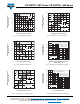
I
FM
t
rr
dir
dt
I
RM(REC)
Q
rr
t
t
a
t
b
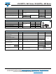
THERMAL - MECHANICAL SPECIFICATIONS
PARAMETER SYMBOL TEST CONDITIONS VALUES UNITS
Maximum junction and storage
temperature range
T
J
, T
Stg
- 40 to 150 °C
Maximum thermal resistance,
junction to case
R
thJC
DC operation 0.9
°C/W
Maximum thermal resistance,
junction to ambient
R
thJA
62
Typical thermal resistance,
case to heatsink
R
thCS
Mounting surface, smooth and greased 0.5
Approximate weight
2g
0.07 oz.
Mounting torque
minimum 6 (5)
kgf · cm
(lbf · in)
maximum 12 (10)
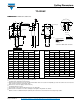
Marking device Case style TO-220AC
20ETF02
20ETF04
20ETF06