
Datasheet


VS-15ETL06PbF, VS-15ETL06-N3, VS-15ETL06FPPbF, VS-15ETL06FP-N3
www.vishay.com
Vishay Semiconductors
Revision: 02-Jan-12
3
Document Number: 94004
For technical questions within your region: DiodesAmericas@vishay.com
, DiodesAsia@vishay.com, DiodesEurope@vishay.com
THIS DOCUMENT IS SUBJECT TO CHANGE WITHOUT NOTICE. THE PRODUCTS DESCRIBED HEREIN AND THIS DOCUMENT
ARE SUBJECT TO SPECIFIC DISCLAIMERS, SET FORTH AT www.vishay.com/doc?91000
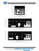
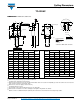
Fig. 3 - Typical Junction Capacitance vs. Reverse Voltage
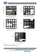
Fig. 4 - Maximum Thermal Impedance Z
thJC
Characteristics
Fig. 5 - Maximum Thermal Impedance Z
thJC
Characteristics (FULL-PAK)
100
10
0 100 200 300 400 500 600
C
T
- Junction Capacitance (pF)
V
R
- Reverse Voltage (V)
T
J
= 25 °C
0.01
0.1
1
10
0.00001 0.0001 0.001 0.01 0.1 1
t
1
- Rectangular Pulse Duration (s)
Z
thJC
- Thermal Impedance (°C/W)
Single pulse
(thermal resistance)
.
.
P
DM
t
1
t
2
Notes:
1. Duty factor D = t
1
/t
2
2. Peak T
J
= P
DM
x Z
thJC
+ T
C
10
D = 0.50
D = 0.20
D = 0.10
D = 0.05
D = 0.02
D = 0.01
0.01
0.1
1
10
0.00001 0.0001 0.001 0.01 0.1 1
t
1
- Rectangular Pulse Duration (s)
Z
thJC
- Thermal Impedance (°C/W)
Single pulse
(thermal resistance)
.
.
P
DM
t
1
t
2
Notes:
1. Duty factor D = t
1
/t
2
2. Peak T
J
= P
DM
x Z
thJC
+ T
C
10
100
D = 0.50
D = 0.20
D = 0.10
D = 0.05
D = 0.02
D = 0.01