
Datasheet

VS-12TQ035SPbF, VS-12TQ040SPbF, VS-12TQ045SPbF
www.vishay.com
Vishay Semiconductors
Revision: 23-May-14
3
Document Number: 94138
For technical questions within your region: DiodesAmericas@vishay.com
, iodesAsia@vishay.com, DiodesEurope@vishay.com
THIS DOCUMENT IS SUBJECT TO CHANGE WITHOUT NOTICE. THE PRODUCTS DESCRIBED HEREIN AND THIS DOCUMENT
ARE SUBJECT TO SPECIFIC DISCLAIMERS, SET FORTH AT www.vishay.com/doc?91000
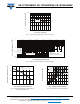
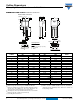
Fig. 3 - Typical Junction Capacitance vs. Reverse Voltage
Fig. 4 - Maximum Thermal Impedance Z
thJC
Characteristics
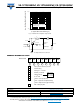
Fig. 5 - Maximum Allowable Case Temperature vs.
Average Forward Current
Fig. 6 - Forward Power Loss Characteristics
C
T
- Junction Capacitance (pF)
V
R
- Reverse Voltage (V)
0 20304050
100
1000
10
T
J
= 25 °C
Z
thJC
- Thermal Impedance (°C/W)
0.001
0.01
0.1
1
10
D = 0.50
D = 0.33
D = 0.25
D = 0.17
D = 0.08
t
1
- Rectangular Pulse Duration (s)
0.00001 0.0001 0.001 0.01 0.1 1 10 100
Single pulse
(thermal resistance)
.
.
P
DM
t
1
t
2
Notes:
1. Duty factor D = t
1
/t
2
2. Peak T
J
= P
DM
x Z
thJC
+ T
C
Allowable Case Temperature (°C)
I
F(AV)
- Average Forward Current (A)
016248
115
125
135
145
155
DC
41220
12TQ
R
thJC
(DC) = 2.0 °C/W
0
4
8
12
Average Power Loss (W)
I
F(AV)
- Average Forward Current (A)
0
81622
10
6
2
642
10 12 14
18 20
D = 0.08
D = 0.17
D = 0.25
D = 0.33
D = 0.50
RMS limit
DC