
Datasheet

VS-12F(R) Series
www.vishay.com
Vishay Semiconductors
Revision: 28-Jan-14
4
Document Number: 93487
For technical questions within your region: DiodesAmericas@vishay.com
, DiodesAsia@vishay.com, DiodesEurope@vishay.com
THIS DOCUMENT IS SUBJECT TO CHANGE WITHOUT NOTICE. THE PRODUCTS DESCRIBED HEREIN AND THIS DOCUMENT
ARE SUBJECT TO SPECIFIC DISCLAIMERS, SET FORTH AT www.vishay.com/doc?91000
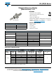
Fig. 5 - Maximum Non-Repetitive Surge Current
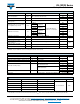
Fig. 6 - Maximum Non-Repetitive Surge Current
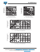
Fig. 7 - Forward Voltage Drop Characteristics
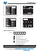
Fig. 8 - Thermal Impedance Z
thJC
Characteristics
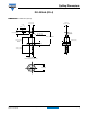
ORDERING INFORMATION TABLE
100
125
150
175
200
225
250
1 10 100
Peak Half Sine Wave Forward Current (A)
Number Of Equal Amplitude Half Cycle Current Pulses (N)
12F(R) Series
Initial T = 175°C
@ 60 Hz 0.0083 s
@ 50 Hz 0.0100 s
J
At Any Rated Load Condition And With
Rated V Applied Following Surge.
RRM
100
125
150
175
200
225
250
275
0.01 0.1 1
Peak Half Sine Wave Forward Current (A)
Pulse Train Duration (s)
12F(R) Series
Initial T = 175°C
No Voltage Reapplied
Rated V Reapplied
RRM
J
Versus Pulse Train Duration.
Maximum Non Repetitive Surge Current
1
10
100
1000
0 1 2 3 4 5 6
T = 25°C
J
Instantaneous Forward Current (A)
Instantaneous Forward Voltage (V)
12F(R) Series
T = 175°C
J
Z
thJC
-
Transient Thermal Impedance (°C/W)
0.1
1
10
0.001 0.01 0.1 1 10
Square Wave Pulse Duration (s)
12F(R) Series
Steady State Value
R = 2.0 K/W
(DC Operation)
thJC
LINKS TO RELATED DOCUMENTS
Dimensions www.vishay.com/doc?95311
1
- Current rating: Code = I
F(AV)
2
- F = Standard device
3
- None = Stud normal polarity (cathode to stud)
R = Stud reverse polarity (anode to stud)
4
- Voltage code x 10 = V
RRM
(see Voltage Ratings table)
5
6
- None = Stud base DO-203AA (DO-4) 10-32UNF-2A
M = Stud base DO-203AA (DO-4) M5 x 0.8
(not available for avalanche diodes)
Device code
5 61 32 4
12VS- F R 120 M
- Vishay Semiconductors product