
Datasheet


VOH1016AB, VOH1016AD, VOH1016AG
www.vishay.com
Vishay Semiconductors
Rev. 1.2, 06-Mar-2019
3
Document Number: 84896
For technical questions, contact: optocoupleranswers@vishay.com
THIS DOCUMENT IS SUBJECT TO CHANGE WITHOUT NOTICE. THE PRODUCTS DESCRIBED HEREIN AND THIS DOCUMENT
ARE SUBJECT TO SPECIFIC DISCLAIMERS, SET FORTH AT www.vishay.com/doc?91000
Note
• Minimum and maximum values are testing requirements. Typical values are characteristics of the device and are the result of engineering
evaluation. Typical values are for information only and are not part of the testing requirements
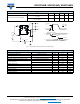
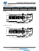
Fig. 3 - Test Circuit for t
on
, t
off
, t
r
, and t
f
ELECTRICAL CHARACTERISTICS (T
amb
= 25 °C, unless otherwise specified)
PARAMETER TEST CONDITION SYMBOL MIN. TYP. MAX. UNIT
INPUT
Forward voltage
I
F
= 4 mA
V
F
-1.11.4
V
I
F
= 0.3 mA 0.7 1.0 -
Reverse current V
R
= 3 V I
R
- - 10 μA
Input capacitance f = 1 MHz, V
F
= 0 V C
IN
- 30 250 pF
OUTPUT
Supply voltage V
CC
3-15V
High level supply current I
F
= 0 mA, V
CC
= 5 V I
CCH
- 0.55 1.0 mA
Low level supply current I
F
= 4 mA, V
CC
= 5 V I
CCL
- 0.55 1.0 mA
High level output current V
CC
= V
O
= 15 V, I
F
= 0 mA I
OH
- - 100 μA
Low level output voltage V
CC
= 5 V, I
F
= 4 mA, I
OL
= 16 mA V
OL
-0.20.4V
Turn-On threshold current V
CC
= 5 V, R
L
= 280 Ω I
F(on)
- 0.65 2.0 mA
Turn-Off threshold current V
CC
= 5 V, R
L
= 280 Ω I
F(off)
0.4 0.6 - mA
Hysteresis ratio V
CC
= 5 V, R
L
= 280 Ω I
F(off)
/I
F(on)
0.5 0.9 0.95
SWITCHING CHARACTERISTICS (T
amb
= 25 °C, unless otherwise specified)
PARAMETER TEST CONDITION SYMBOL MIN. TYP. MAX. UNIT
Propagation delay time to high output level
R
L
= 280 Ω, V
CC
= 5 V,
I
F
= 4 mA
t
PLH
-0.252 μs
Propagation delay time to low output level t
PHL
- 0.05 1.2 μs
Rise time t
r
- 0.05 0.5 μs
Fall time t
f
- 0.04 0.5 μs
Data rate -2-MHz
t
r
= t
f
≤ 0.01 μs
Z = 50 Ω
I
F
5 V
0.1 μF
C
R
E
V
O
V
IN
R
L
270 Ω
I
CC
t
f
t
PLH
50 %
10 %
90 %
V
O
t
PHL
t
r
V
IN
= 5 V
6
5
4
1
2
3