
Datasheet


VOH1016AB, VOH1016AD, VOH1016AG
www.vishay.com
Vishay Semiconductors
Rev. 1.2, 06-Mar-2019
2
Document Number: 84896
For technical questions, contact: optocoupleranswers@vishay.com
THIS DOCUMENT IS SUBJECT TO CHANGE WITHOUT NOTICE. THE PRODUCTS DESCRIBED HEREIN AND THIS DOCUMENT
ARE SUBJECT TO SPECIFIC DISCLAIMERS, SET FORTH AT www.vishay.com/doc?91000
Note
• Stresses in excess of the absolute maximum ratings can cause permanent damage to the device. Functional operation of the device is not
implied at these or any other conditions in excess of those given in the operational sections of this document. Exposure to absolute
maximum ratings for extended periods of the time can adversely affect reliability
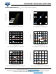
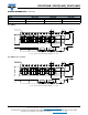
Fig. 1 - Forward Current vs. Ambient Temperature Fig. 2 - Power Dissipation vs. Ambient Temperature
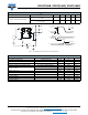
TRUTH TABLE (positive logic)
LED OUTPUT
On L
Off H
ABSOLUTE MAXIMUM RATINGS (T
amb
= 25 °C, unless otherwise specified)
PARAMETER CONDITIONS SYMBOL VALUE UNIT
INPUT
Forward current I
F
50 mA
Reverse voltage V
R
6V
Power dissipation P
diss
120 mW
OUTPUT
Supply voltage V
CC
16 V
Output voltage V
O
V
CC
V
Output current I
O
50 mA
Power dissipation P
diss
130 mW
COUPLER
Power dissipation P
diss
250 mW
Storage temperature T
stg
-55 to +150 °C
Operating temperature T
amb
-40 to +100 °C
Solder temperature For 10 s T
sld
260 °C
10
100
1000
10000
0
10
20
30
40
50
60
-40-20 0 20406080100
Axis Title
1st line
2nd line
2nd line
I
F
- Forward Current (mA)
T
amb
- Ambient Temperature (°C)
10
100
1000
10000
0
50
100
150
200
250
300
-40-20 0 20406080100
Axis Title
1st line
2nd line
2nd line
P
diss
- Power Dissipation (mW)
T
amb
- Ambient Temperature (°C)
Total
Output