
Datasheet


VO615A
www.vishay.com
Vishay Semiconductors
Rev. 2.3, 08-Feb-17
2
Document Number: 81753
For technical questions, contact: optocoupleranswers@vishay.com
THIS DOCUMENT IS SUBJECT TO CHANGE WITHOUT NOTICE. THE PRODUCTS DESCRIBED HEREIN AND THIS DOCUMENT
ARE SUBJECT TO SPECIFIC DISCLAIMERS, SET FORTH AT www.vishay.com/doc?91000
Notes
• Stresses in excess of the absolute maximum ratings can cause permanent damage to the device. Functional operation of the device is not
implied at these or any other conditions in excess of those given in the operational sections of this document. Exposure to absolute
maximum ratings for extended periods of the time can adversely affect reliability
(1)
Refer to reflow profile for soldering conditions for surface mounted devices (SMD), and wave profile for soldering conditions for through hole
devices (DIP), please go to “Assembly Instructions” (www.vishay.com/doc?80054)
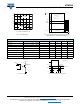
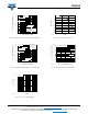
Fig. 1 - Permissible Power Dissipation vs. Ambient Temperature
Note
• Minimum and maximum values are testing requirements. Typical values are characteristics of the device and are the result of engineering
evaluation. Typical values are for information only and are not part of the testing requirements
ABSOLUTE MAXIMUM RATINGS (T
amb
= 25 °C, unless otherwise specified)
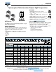
PARAMETER TEST CONDITION SYMBOL VALUE UNIT
INPUT
Reverse voltage V
R
6V
Forward current I
F
60 mA
Forward surge current t
p
≤ 10 μs I
FSM
1.5 A
LED power dissipation at 25 °C P
diss
100 mW
OUTPUT
Collector emitter voltage V
CEO
70 V
Emitter collector voltage V
ECO
7V
Collector current I
C
50 mA
Collector peak current t
p
/T = 0.5, t
p
≤ 10 ms I
CM
100 mA
Output power dissipation at 25 °C P
diss
150 mW
COUPLER
Operating ambient temperature range T
amb
-55 to +110 °C
Storage temperature range T
stg
-55 to +125 °C
Soldering temperature
(1)
2 mm from case, ≤ 10 s T
sld
260 °C
0
50
100
150
200
0 255075100125150
P
tot
- Power Dissipation (mW)
Phototransistor
Diode
T
amb
- Ambient Temperature (°C)
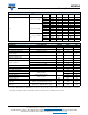
ELECTRICAL CHARACTERISTICS (T
amb
= 25 °C, unless otherwise specified)
PARAMETER TEST CONDITION SYMBOL MIN. TYP. MAX. UNIT
INPUT
Forward voltage I
F
= 50 mA V
F
- 1.43 1.6 V
Reverse current V
R
= 6 V I
R
- - 100 μA
Junction capacitance V
R
= 0, f = 1 MHz C
j
-50-pF
OUTPUT
Collector emitter voltage I
C
= 1 mA V
CEO
70 - - V
Emitter collector voltage I
E
= 100 μA V
ECO
7--V
Collector emitter leakage current V
CE
= 20 V, I
F
= 0 I
CEO
- 10 100 nA
COUPLER
Collector emitter saturation voltage I
F
= 10 mA, I
C
= 1 mA V
CEsat
--0.3V
Cut-off frequency V
CE
= 5 V, I
F
= 10 mA, R
L
= 100 Ω f
c
- 110 - kHz
Coupling capacitance f = 1 MHz C
k
-0.6-pF