
Datasheet

VLMO21.., VLMS21.., VLMY21..
www.vishay.com
Vishay Semiconductors
Rev. 1.5, 28-Nov-14
7
Document Number: 81233
For technical questions, contact: LED@vishay.com
THIS DOCUMENT IS SUBJECT TO CHANGE WITHOUT NOTICE. THE PRODUCTS DESCRIBED HEREIN AND THIS DOCUMENT
ARE SUBJECT TO SPECIFIC DISCLAIMERS, SET FORTH AT www.vishay.com/doc?91000
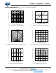
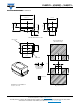
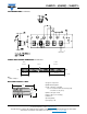
PACKAGE DIMENSIONS in millimeters
Drawing-No.: 6.541-5069.01-4
Issue: 2; 24.11.14
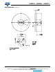
2.2 ± 0.1
2.05 ± 0.1
0.4 ± 0.1
0.1 ± 0.05
0.7 ± 0.1
1.3 ± 0.1
0.9 ± 0.1
1.4 ± 0.1
(1.2)
Cathode mark
Not indicated tolerances ± 0.2
(1.5)
(0.9)
Area not at
technical drawings
according to DIN
specications
Solder resist
Cu.area > 5 mm
2
1
0.8 0.8
2.8
Proposed pad layout
(for reference only)