
Datasheet


VCNL36687S
www.vishay.com
Vishay Semiconductors
Rev. 1.2, 21-Sep-2018
7
Document Number: 84907
For technical questions, contact: sensorstechsupport@vishay.com
THIS DOCUMENT IS SUBJECT TO CHANGE WITHOUT NOTICE. THE PRODUCTS DESCRIBED HEREIN AND THIS DOCUMENT
ARE SUBJECT TO SPECIFIC DISCLAIMERS, SET FORTH AT www.vishay.com/doc?91000
APPLICATION INFORMATION
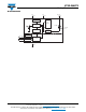
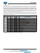
Pin Connection with the Host
VCNL36687S integrates proximity sensor and VCSEL all together with an I
2
C interface. It is easy for the baseband (CPU) to
access PS output data via I
2
C interface without additional software algorithms. The hardware schematic is shown in the
following diagram.
Two additional capacitors in the circuit can be used for the following purposes: (1) the 1 μF capacitor near the V
DD
pin is used
for power supply noise rejection, (2) the 1 μF capacitor is used to prevent the VCSEL voltage from instantly dropping when the
VCSEL is turned on, and (3) 2.2 kΩ is suitable for the pull up resistor of I
2
C except for the 10 kΩ applied on the INT pin.
Fig. 8 - Hardware Pin Connection Diagram
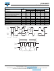
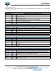
Digital Interface
VCNL36687S applies single slave address 0x60 (HEX) of 7-bit addressing following I
2
C protocol. All operations can be
controlled by the command register. The simple command structure helps users easily program the operation setting and latch
the light data from VCNL36687S. As Fig. 9 shows, VCNL36687S’s I
2
C command format is simple for read and write operations
between VCNL36687S and the host. The white sections indicate host activity and the gray sections indicate VCNL36687S’s
acknowledgement of the host access activity. Write word and read word protocol is suitable for accessing registers particularly
for 12-bit PS data. Interrupt can be cleared by reading data out from register: INT_Flag. All command codes should follow read
word and write word protocols.
Fig. 9 - Write Word and Read Word Protocol
V
DD
GPIO INT
SCL
8
7
3
5
1
1 μF
GND
SDA
SCL
SDA
6
2.2 kΩ2.2 kΩ
V
VCSEL
10 kΩ
V
pull_up
Cathode
Anode
4
2
VCNL36687S
Baseband
V
DD
V
PP
1 μF
S Slave address Wr A Command code A Data byte low A Data byte high A
17 811 1
81 8
P
11
Send word → write command to VCNL36687S
1
Slave address
7
Wr A Command code A S Slave address Rd A Data byte low A Data byte high N P
11 8 11 7 11 8 1 8 1 1
S
Receive word → read data from VCNL36687S
S = start condition
P = stop condition
A = acknowledge
N = not acknowledge
Host action
VCNL36687S response