
Datasheet


VCNL36687S
www.vishay.com
Vishay Semiconductors
Rev. 1.2, 21-Sep-2018
4
Document Number: 84907
For technical questions, contact: sensorstechsupport@vishay.com
THIS DOCUMENT IS SUBJECT TO CHANGE WITHOUT NOTICE. THE PRODUCTS DESCRIBED HEREIN AND THIS DOCUMENT
ARE SUBJECT TO SPECIFIC DISCLAIMERS, SET FORTH AT www.vishay.com/doc?91000
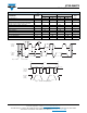
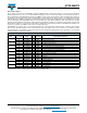
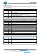
Fig. 1 - I
2
C Bus Timing Diagram
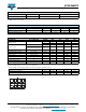
I
2
C BUS TIMING CHARACTERISTICS (T
amb
= 25 °C, unless otherwise specified)
PARAMETER SYMBOL
STANDARD MODE FAST MODE
UNIT
MIN. MAX. MIN. MAX.
Clock frequency f
(I2CCLK)
10 100 10 400 kHz
Bus free time between start and stop condition t
(BUF)
4.7 - 1.3 - μs
Hold time after (repeated) start condition;
after this period, the first clock is generated
t
(HDSTA)
4.0 - 0.6 - μs
Repeated start condition setup time t
(SUSTA)
4.7 - 0.6 - μs
Stop condition setup time t
(SUSTO)
4.0 - 0.6 - μs
Data hold time t
(HDDAT)
- 3450 - 900 ns
Data setup time t
(SUDAT)
250 - 100 - ns
I
2
C clock (SCK) low period t
(LOW)
4.7 - 1.3 - μs
I
2
C clock (SCK) high period t
(HIGH)
4.0 - 0.6 - μs
Clock / data fall time t
(f)
- 300 - 300 ns
Clock / data rise time t
(r)
- 1000 - 300 ns
V
IH
V
IH
t
(LOW)
V
IL
t
(f)
t
(HIGH)
t
(SUDAT)
{{
P
Stop condition
S
Start condition
{{
PS
Start Stop
I
2
C BUS
CLOCK
(SCLK)
I
2
C BUS
DATA
(SDAT)
I
2
C BUS
CLOCK
(SCLK)
I
2
C BUS
DATA
(SDAT)
t
(r)
t
(HDSTA)
t
(HDDAT)
V
IL
t
(BUF)
t
(SUSTA)
t
(SUSTO)
t
(LOSEXT)
t
(LOWMEXT)
t
(LOWMEXT)
SCLK
ACK
SDA
ACK
t
(LOWMEXT)