
Datasheet


TCUT1350X01
www.vishay.com
Vishay Semiconductors
Rev. 1.0, 14-Mar-13
2
Document Number: 84816
For technical questions, contact: sensorstechsupport@vishay.com
THIS DOCUMENT IS SUBJECT TO CHANGE WITHOUT NOTICE. THE PRODUCTS DESCRIBED HEREIN AND THIS DOCUMENT
ARE SUBJECT TO SPECIFIC DISCLAIMERS, SET FORTH AT www.vishay.com/doc?91000
ABSOLUTE MAXIMUM RATINGS
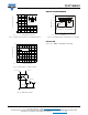
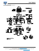
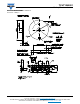
Fig. 1 - Power Dissipation Limit vs. Ambient Temperature Fig. 2 - Forward Current Limit vs. Ambient Temperature
ABSOLUTE MAXIMUM RATINGS (T
amb
= 25 °C, unless otherwise specified)
PARAMETER TEST CONDITION SYMBOL VALUE UNIT
COUPLER
Total power dissipation T
amb
125 °C P
tot
37.5 mW
Junction temperature T
j
140 °C
Ambient temperature range T
amb
- 40 to + 125 °C
Storage temperature range T
stg
- 40 to + 125 °C
Soldering temperature In accordance with fig. 16 T
sd
260 °C
INPUT (EMITTER)
Reverse voltage V
R
5V
Forward current T
amb
125 °C I
F
25 mA
Forward surge current t
p
10 μs I
FSM
200 mA
Power dissipation T
amb
125 °C P
V
37.5 mW
OUTPUT (DETECTOR)
Collector emitter voltage V
CEO
20 V
Emitter collector voltage V
ECO
7V
Collector current I
C
20 mA
Collector dark current T
amb
85 °C, V
CE
= 5 V I
CEO
3.3 μA
0
5
10
15
20
25
30
35
40
0 20 40 60 80 100 140
P
V
- Power Dissipation (mW)
T
amb
- Ambient Temperature (°C)
R
thJA
= 460 K/W
120
0
5
10
15
20
25
30
0 20 40 60 80 100 140
I
F
- Forward Current (mA)
T
amb
- Ambient Temperature (°C)
R
thJA
= 460 K/W
120