
Datasheet


TCST1103, TCST1202, TCST1300
www.vishay.com
Vishay Semiconductors
Rev. 2.0, 24-Aug-11
2
Document Number: 83764
For technical questions, contact: sensorstechsupport@vishay.com
THIS DOCUMENT IS SUBJECT TO CHANGE WITHOUT NOTICE. THE PRODUCTS DESCRIBED HEREIN AND THIS DOCUMENT
ARE SUBJECT TO SPECIFIC DISCLAIMERS, SET FORTH AT www.vishay.com/doc?91000
ABSOLUTE MAXIMUM RATINGS
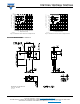
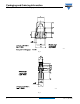
Fig. 1 - Power Dissipation Limit vs. Ambient Temperature
INPUT (EMITTER)
Reverse voltage V
R
6V
Forward current I
F
60 mA
Forward surge current t
p
≤ 10 μs I
FSM
3A
Power dissipation T
amb
≤ 25 °C P
V
100 mW
Junction temperature T
j
100 °C
OUTPUT (DETECTOR)
Collector emitter voltage V
CEO
70 V
Emitter collector voltage V
ECO
7V
Collector peak current t
p
/T = 0.5, t
p
≤ 10 ms I
CM
200 mA
Power dissipation T
amb
≤ 25 °C P
V
150 mW
Junction temperature T
j
100 °C
ABSOLUTE MAXIMUM RATINGS (T
amb
= 25 °C, unless otherwise specified)
PARAMETER TEST CONDITION SYMBOL VALUE UNIT
0
0
100
200
300
400
95 11088
P - Power Dissipation (mW)
T
amb
- Ambient Temperature (°C)
Coupled device
Phototransistor
IR-diode
150 120 90 60
30
BASIC CHARACTERISTICS (T
amb
= 25 °C, unless otherwise specified)
PARAMETER TEST CONDITION PART SYMBOL MIN. TYP. MAX. UNIT
COUPLER
Current transfer ratio V
CE
= 5 V, I
F
= 20 mA
TCST1103 CTR 10 20 %
TCST1202 CTR 5 10 %
TCST1300 CTR 1.25 2.5 %
Collector current V
CE
= 5 V, I
F
= 20 mA
TCST1103 I
C
24 mA
TCST1202 I
C
12 mA
TCST1300 I
C
0.25 0.5 mA
Collector emitter saturation
voltage
I
F
= 20 mA, I
C
= 1 mA TCST1103 V
CEsat
0.4 V
I
F
= 20 mA, I
C
= 0.5 mA TCST1202 V
CEsat
0.4 V
I
F
= 20 mA, I
C
= 0.1 mA TCST1300 V
CEsat
0.4 V
Resolution, path of the shutter
crossing the radiant sensitive
zone
I
Crel
= 10 % to 90 %
TCST1103 s 0.6 mm
TCST1202 s 0.4 mm
TCST1300 s 0.2 mm