
Datasheet


TCMT110. Series
www.vishay.com
Vishay Semiconductors
Rev. 3.1, 25-Jun-2018
4
Document Number: 83510
For technical questions, contact: optocoupleranswers@vishay.com
THIS DOCUMENT IS SUBJECT TO CHANGE WITHOUT NOTICE. THE PRODUCTS DESCRIBED HEREIN AND THIS DOCUMENT
ARE SUBJECT TO SPECIFIC DISCLAIMERS, SET FORTH AT www.vishay.com/doc?91000
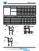
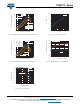
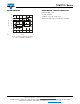
TYPICAL CHARACTERISTICS (T
amb
= 25 °C, unless otherwise specified)
Fig. 4 - Total Power Dissipation vs. Ambient Temperature Fig. 5 - Forward Voltage vs. Forward Current
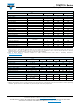
SAFETY AND INSULATION RATINGS
PARAMETER TEST CONDITION SYMBOL VALUE UNIT
Climatic classification According to IEC 68 part 1 40 / 110 / 21
Pollution degree According to DIN VDE 0109 2
Comparative tracking index Insulation group IIIa CTI 175
Maximum rated withstanding isolation voltage According to UL1577, t = 1 min V
ISO
3750 V
RMS
Maximum transient isolation voltage According to DIN EN 60747-5-5 V
IOTM
6000 V
peak
Maximum repetitive peak isolation voltage According to DIN EN 60747-5-5 V
IORM
707 V
peak
Isolation resistance
T
amb
= 25 °C, V
IO
= 500 V
R
IO
≥ 10
12
ΩT
amb
= 100 °C, V
IO
= 500 V ≥ 10
11
T
amb
= T
S
, V
IO
= 500 V ≥ 10
9
Output safety power P
SO
350 mW
Input safety current I
SI
150 mA
Input safety temperature T
S
175 °C
Creepage distance ≥ 5mm
Clearance distance ≥ 5mm
Insulation thickness DTI ≥ 0.4 mm
Input to output test voltage, method B
V
IORM
x 1.875 = V
PR
, 100 % production test
with t
M
= 1 s, partial discharge < 5 pC
V
PR
1326 V
peak
Input to output test voltage, method A
V
IORM
x 1.6 = V
PR
, 100 % sample test
with t
M
= 10 s, partial discharge < 5 pC
V
PR
1132 V
peak
0
50
100
150
200
250
300
04080120
P
tot
- Total Power Dissipation (mW)
T
amb
- Ambient Temperature (°C)
96 11700
Coupled device
Phototransistor
IR-diode
0.1
1
10
100
0.6 0.8 1.0 1.2 1.4 1.6
I
F
- Forward Current (mA)
V
F
- Forward Voltage (V)
T
amb
= 110 °C
T
amb
= 75 °C
T
amb
= 25 °C
T
amb
= 0 °C
T
amb
= -55 °C