
Datasheet


TCLT10.. Series
Document Number 83515
Rev. 2.0, 27-Sep-05
Vishay Semiconductors
www.vishay.com
5
Switching Characteristics
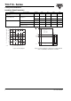
Parameter Test condition Symbol Min Typ. Max Unit
Delay time V
S
= 5 V, I
C
= 2 mA, R
L
= 100 Ω
(see figure 3)
t
d
3.0 µs
Rise time V
S
= 5 V, I
C
= 2 mA, R
L
= 100 Ω
(see figure 3)
t
r
3.0 µs
Turn-on time V
S
= 5 V, I
C
= 2 mA, R
L
= 100 Ω
(see figure 3)
t
on
6.0 µs
Storage time V
S
= 5 V, I
C
= 2 mA, R
L
= 100 Ω
(see figure 3)
t
s
0.3 µs
Fall time V
S
= 5 V, I
C
= 2 mA, R
L
= 100 Ω
(see figure 3)
t
f
4.7 µs
Turn-off time V
S
= 5 V, I
C
= 2 mA, R
L
= 100 Ω
(see figure 3)
t
off
5.0 µs
Turn-on time V
S
= 5 V, I
F
= 10 mA, R
L
= 1 kΩ
(see figure 4)
t
on
9.0 µs
Turn-off time V
S
= 5 V, I
F
= 10 mA, R
L
= 1 kΩ
(see figure 4)
t
off
10.0 µs
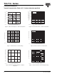
Figure 3. Test circuit, non-saturated operation
Figure 4. Test circuit, saturated operation
Channel I
Channel II
95 10804
R
G
= 50 W
t
p
t
p
= 50 Ps
T
= 0.01
+ 5 V
I
F
0
50 W 100 W
I
F
I
C
= 2 mA;
adjusted through
input amplitude
Oscilloscope
R
L
= 1 MW
C
L
= 20 pF
Channel I
Channel II
95 10843
R
G
=50
Ω
t
p
t
p
=50 s
T
= 0.01
+5V
I
C
I
F
0
50
1k
I
F
=10mA
Oscilloscope
R
L
≥
C
L
20 pF
Ω
M1
≤
µ
Ω
Ω
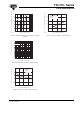
Figure 5. Switching Times
t
p
t
t
0
0
10%
90%
100%
t
r
t
d
t
on
t
s
t
f
t
off
I
F
I
C
96 11698
t
p
pulse duration
t
d
delay time
t
r
rise time
t
on
(= t
d
+t
r
) turn-on time
t
s
storage time
t
f
fall time
t
off
(= t
s
+t
f
) turn-off time