
Datasheet


www.vishay.com
2
Document Number 83515
Rev. 2.0, 27-Sep-05
TCLT10.. Series
Vishay Semiconductors
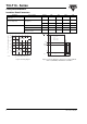
Absolute Maximum Ratings
T
amb
= 25 °C, unless otherwise specified
Stresses in excess of the absolute Maximum Ratings can cause permanent damage to the device. Functional operation of the device is
not implied at these or any other conditions in excess of those given in the operational sections of this document. Exposure to absolute
Maximum Rating for extended periods of the time can adversely affect reliability.
Input
Output
Coupler
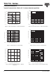
Electrical Characteristics
T
amb
= 25 °C, unless otherwise specified
Minimum and maximum values are testing requirements. Typical values are characteristics of the device and are the result of engineering
evaluation. Typical values are for information only and are not part of the testing requirements.
Input
Output
Parameter Test condition Symbol Value Unit
Reverse voltage V
R
6V
Forward current I
F
60 mA
Forward surge current t
p
≤ 10 µsI
FSM
1.5 A
Power dissipation P
diss
100 mW
Junction temperature T
j
125 °C
Parameter Test condition Symbol Value Unit
Collector emitter voltage V
CEO
70 V
Emitter collector voltage V
ECO
7V
Collector current I
C
50 mA
Collector peak current t
p
/T = 0.5, t
p
≤ 10 ms I
CM
100 mA
Power dissipation P
diss
150 mW
Junction temperature T
j
125 °C
Parameter Test condition Symbol Value Unit
Isolation test voltage (RMS) V
ISO
5000 V
RMS
Total power dissipation P
tot
250 mW
Operating ambient temperature
range
T
amb
- 40 to + 100 °C
Storage temperature range T
stg
- 40 to + 100 °C
Soldering temperature T
sld
240 °C
Parameter Test condition Symbol Min Typ. Max Unit
Forward voltage I
F
= ± 50 mA V
F
1.25 1.6 V
Junction capacitance V
R
= 0 V, f = 1 MHz C
j
50 pF
Parameter Test condition Symbol Min Typ. Max Unit
Collector emitter voltage I
C
= 1 mA V
CEO
70 V
Emitter collector voltage I
E
= 100 µAV
ECO
7V
Collector-emitter cut-off current V
CE
= 20 V, I
f
= 0, E = 0 I
CEO
10 100 nA