
Datasheet

SS2H9, SS2H10
www.vishay.com
Vishay General Semiconductor
Revision: 21-Jul-17
1
Document Number: 88750
For technical questions within your region: DiodesAmericas@vishay.com
, DiodesAsia@vishay.com, DiodesEurope@vishay.com
THIS DOCUMENT IS SUBJECT TO CHANGE WITHOUT NOTICE. THE PRODUCTS DESCRIBED HEREIN AND THIS DOCUMENT
ARE SUBJECT TO SPECIFIC DISCLAIMERS, SET FORTH AT www.vishay.com/doc?91000
High Voltage Surface Mount Schottky Rectifier
High Barrier Technology for Improved High Temperature Performance
FEATURES
• Low profile package
• Guardring for overvoltage protection
• Ideal for automated placement
• Low power losses, high efficiency
• Low forward voltage drop
• Low leakage current
• High surge capability
• Meets MSL level 1, per J-STD-020, LF maximum peak of
260 °C
• AEC-Q101 qualified available
- Automotive ordering code: base P/NHE3 or P/NHM3
• Material categorization: for definitions of compliance
please see www.vishay.com/doc?99912
TYPICAL APPLICATIONS
For use in low voltage high frequency inverters,
freewheeling, DC/DC converters, and polarity protection
applications.
MECHANICAL DATA
Case: SMB (DO-214AA)
Molding compound meets UL 94 V-0 flammability rating
Base P/N-E3 - RoHS-compliant, commercial grade
Base P/N-M3 - halogen-free, RoHS-compliant, commercial
grade
Base P/NHE3_X - RoHS-compliant and AEC-Q101 qualified
Base P/NHM3_X - halogen-free, RoHS-compliant, and
AEC-Q101 qualified
(“_X” denotes revision code e.g. A, B, .....)
Terminals: matte tin plated leads, solderable per
J-STD-002 and JESD 22-B102
E3, M3, HE3, and HM3 suffix meets JESD 201 class 2
whisker test
Polarity: color band denotes the cathode end
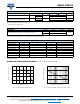
PRIMARY CHARACTERISTICS
I
F(AV)
2.0 A
V
RRM
90 V, 100 V
I
FSM
75 A
V
F
0.65 V
I
R
10 μA
T
J
max. 175 °C
Package SMB (DO-214AA)
Diode variations Single
SMB (DO-214AA)
Available
MAXIMUM RATINGS (T
A
= 25 °C unless otherwise noted)
PARAMETER SYMBOL SS2H9 SS2H10 UNIT
Device marking code MS9 MS10
Maximum repetitive peak reverse voltage V
RRM
90 100 V
Working peak reverse voltage V
RWM
90 100 V
Maximum DC blocking voltage V
DC
90 100 V
Maximum average forward rectified current at: T
L
= 130 °C I
F(AV)
2.0 A
Peak forward surge current 8.3 ms single half sine-wave
superimposed on rated load
I
FSM
75 A
Peak repetitive reverse surge current at t
p
= 2.0 μs, 1 kHz I
RRM
1.0 A
Voltage rate of change (rated V
R
) dV/dt 10 000 V/μs
Operating junction and storage temperature range T
J
, T
STG
-65 to +175 °C