
Datasheet

SMAJ530, SMAJ550
www.vishay.com
Vishay General Semiconductor
Revision: 10-Dec-13
3
Document Number: 88391
For technical questions within your region: DiodesAmericas@vishay.com
, DiodesAsia@vishay.com, DiodesEurope@vishay.com
THIS DOCUMENT IS SUBJECT TO CHANGE WITHOUT NOTICE. THE PRODUCTS DESCRIBED HEREIN AND THIS DOCUMENT
ARE SUBJECT TO SPECIFIC DISCLAIMERS, SET FORTH AT www.vishay.com/doc?91000
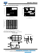
RATINGS AND CHARACTERISTICS CURVES (T
A
= 25 °C unless otherwise noted)
Fig. 1 - Peak Pulse Power Rating Curve
Fig. 2 - Pulse Power or Current vs. Initial Junction Temperature
Fig. 3 - Pulse Waveform
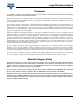
PACKAGE OUTLINE DIMENSIONS in inches (millimeters)
0.1
1
10
100
P
PPM
- Peak Pulse Power (kW)
t
d
- Pulse Width (s)
Non-Repetitive Pulse
Waveform shown in Fig. 3
T
A
= 25 °C
0.1 µs 1.0 µs 10 µs 100 µs 1.0 ms 10 ms
0 255075100
100
75
50
25
0
125 150 175 200
T
J
- Initial Temperature (°C)
Peak Pulse Power (P
PP
) or Current (I
PP
)
Derating in Percentage, %
0
50
100
150
t
r
= 10 µs
Peak Value
I
PPM
Half Value -
I
PPM
I
PP
2
t
d
10/1000 µs Waveform
as defined by R.E.A.
0
1.0
2.0
3.0 4.0
t - Time (ms)
I
PPM
- Peak Pulse Current, % I
RSM
T
J
= 25 °C
Pulse Width (t
d
)
is defined as the Point
where the Peak Current
decays to 50 % of I
PPM
0.008 (0.203)
0.194 (4.93)
0.208 (5.28)
0.157 (3.99)
0.177 (4.50)
0.100 (2.54)
0.110 (2.79)
0.078 (1.98)
0.090 (2.29)
0.006 (0.152)
0.012 (0.305)
0.049 (1.25)
0.065 (1.65)
Cathode Band
0 (0)
DO-214AC (SMA)
Mounting Pad Layout
0.074 (1.88)
MAX.
0.208 (5.28)
REF.
0.066 (1.68)
MIN.
0.060 (1.52)
MIN.
0.030 (0.76)
0.060 (1.52)