
Datasheet
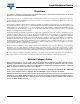

New Product
SM8S10 thru SM8S43A
www.vishay.com
Vishay General Semiconductor
Revision: 14-Sep-11
3
Document Number: 88387
For technical questions within your region: DiodesAmericas@vishay.com
, DiodesAsia@vishay.com, DiodesEurope@vishay.com
THIS DOCUMENT IS SUBJECT TO CHANGE WITHOUT NOTICE. THE PRODUCTS DESCRIBED HEREIN AND THIS DOCUMENT
ARE SUBJECT TO SPECIFIC DISCLAIMERS, SET FORTH AT www.vishay.com/doc?91000
Note
(1)
AEC-Q101 qualified
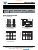
RATINGS AND CHARACTERISTICS CURVES
(T
A
= 25 °C unless otherwise noted)
Fig. 1 - Power Derating Curve
Fig. 2 - Load Dump Power Characteristics
(10 ms Exponential Waveform)
Fig. 3 - Pulse Waveform
Fig. 4 - Reverse Power Capability
THERMAL CHARACTERISTICS (T
C
= 25 °C unless otherwise noted)
PARAMETER SYMBOL VALUE UNIT
Typical thermal resistance, junction to case R
JC
0.90 °C/W
ORDERING INFORMATION (Example)
PREFERRED P/N UNIT WEIGHT (g) PREFERRED PACKAGE CODE BASE QUANTITY DELIVERY MODE
SM8S10AHE3/2D
(1)
2.605 2D 750
13" diameter plastic tape and reel,
anode towards the sprocket hole
0
2.0
4.0
6.0
8.0
0
50
100
150 200
Power Dissipation (W)
Case Temperature (°C)
0
2000
1000
3000
4000
5000
6000
25
50 75
100 125
150 175
Load Dump Power (W)
Case Temperature (°C)
0
50
100
150
0
10
20
30 40
Input Peak Pulse Current (%)
t - Time (ms)
t
d
t
r
= 10 μs
Peak Value
I
PPM
Half Value -
I
PPM
I
PP
2
T
J
= 25 °C
Pulse Width (t
d
) is
Dened as the Point
Where the Peak Current
Decays to 50 % of I
PPM
Reverse Surge Power (W)
1000
10 000
10
100
Pulse Width (ms) - ½ I
PP
Exponential Waveform