
Datasheet

Document Number: 91382 www.vishay.com
S11-0440-Rev. C, 14-Mar-11 5
This datasheet is subject to change without notice.
THE PRODUCT DESCRIBED HEREIN AND THIS DATASHEET ARE SUBJECT TO SPECIFIC DISCLAIMERS, SET FORTH AT
www.vishay.com/doc?91000
SiHG20N50C
Vishay Siliconix
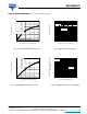
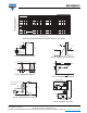
Fig. 10 - Normalized Thermal Transient Impedance, Junction-to-Case (TO-247)
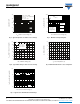
Fig. 11a - Switching Time Test Circuit
Fig. 11b - Switching Time Waveforms
Fig. 12a - Unclamped Inductive Test Circuit
Fig. 12b - Unclamped Inductive Waveforms
Fig. 13a - Basic Gate Charge Waveform
Fig. 13b - Gate Charge Test Circuit
10
-4
10
-3
10
-2
0.1 1
Normalized Effective Transient
Thermal Impedance
0.01
0.1
1
Pulse Time (s)
Single Pulse
0.02
0.05
0.1
0.2
Duty Cycle = 0.5
Pulse width ≤ 1 µs
Duty factor ≤ 0.1 %
R
D
V
GS
R
g
D.U.T.
10 V
+
-
V
DS
V
DD
V
DS
90 %
10 %
V
GS
t
d(on)
t
r
t
d(off)
t
f
R
g
I
AS
0.01 Ω
t
p
D.U.T
L
V
DS
+
-
V
DD
10 V
Vary t
p
to obtain
required I
AS
I
AS
V
DS
V
DD
V
DS
t
p
Q
GS
Q
GD
Q
G
V
G
Charge
10 V
D.U.T.
3 mA
V
GS
V
DS
I
G
I
D
0.3 µF
0.2 µF
50 kΩ
12 V
Current regulator
Current sampling resistors
Same type as D.U.T.
+
-